

PCB assembly
-
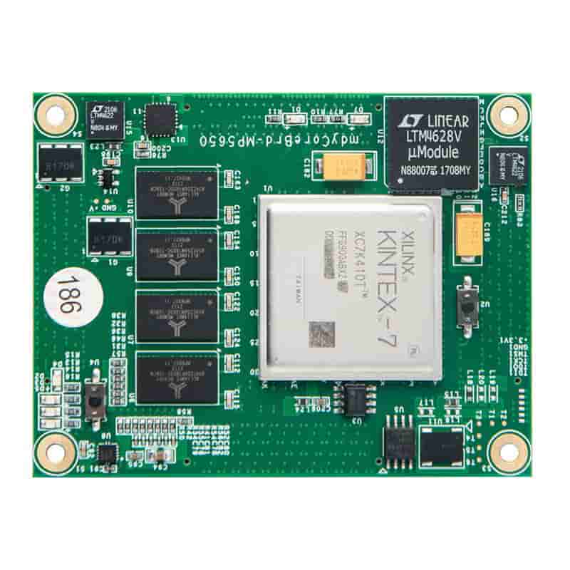
Fpga Xilinx-K7 Kintex7 Xc7k325 410t Industrial Grade
DDR3 SDRAMQ: 16GB DDR3,4GB per piece, 16bit Data Bit Data Bid SPI Flash: One piece of 128MBITQSPIFLASH, which can be used for FPGA configuration files and user data storage FPGA Bank interface levels: adjustable 1.8V, 2.5V, 3.3V electrical If you need to replace the level, you only need to replace the corresponding position of the magnetic bead to achieve adjustment.
-

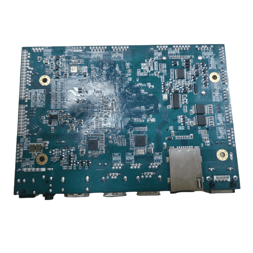
Intelligent media motherboard robot motherboard subway screen main control board display motherboard
Multi -functional intelligent media motherboard MC1001V1 is based on the T3 platform of the full -minded car regulatory chip T3 platform. It is mainly used for the content display and intelligent control of the vehicle LCD display product. It can also be used for smart display terminal products, video terminal products, industrial automation terminal products, etc. Support H.264 hard decoding, Ethernet flow media coding, network linkage control, etc. Data synchronization control adopts the mode of RS485 and Ethernet.
-

Altera image processing HDMI input 4K Gigabit network port DDR3
Hisilicon Hi3536+Altera FPGA Video Development Board HDMI Input 4K Code H.264/265 Gigabit Network Port
-
Android board all -in -one motherboard self -service terminal motherboard
RK3288 Android all -in -one board, using Rocin Micro RK3288 quad -core chip solution to support Google Android4.4 system. RK3288 is the world’s first quad-core ARM new A17 kernel chip in the world the first chip to support the latest super mali-T76X series GPU and the world’s first 4kx2k hard solution H.265 chip. It supports mainstream sound video formats and pictures. decoding. Support the two -screen different display function, Double 8/10 LVDS interface, support 3840*2160, can ... -
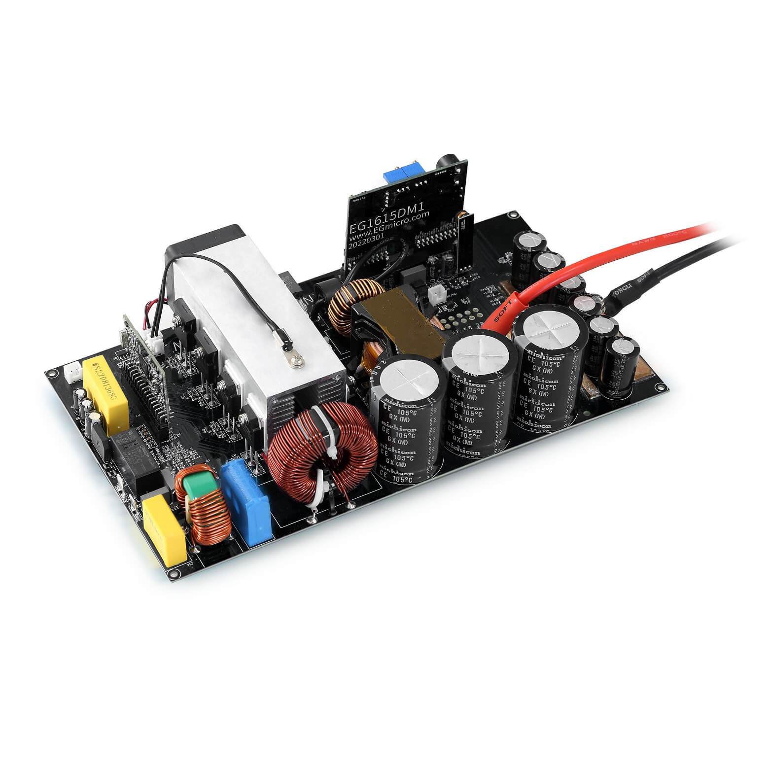
Energy storage inverter PCBA Printed circuit board assembly for energy storage inverters
1. Super fast charging: integrated communication and DC two -way transformation
2. High -efficiency: Adopt advanced technology design, low loss, low heating, saving battery power, extending discharge time
3. Small volume: high power density, small space, low weight, strong structural strength, suitable for portable and mobile applications
4. Good load adaptability: output 100/110/120V or 220/230/240V, 50/60Hz sine wave, strong overload capacity, suitable for various IT devices, electric tools, home appliances, do not pick the load
5. Ultra-wide input voltage frequency range: Extremely wide input voltage 85-300VAC (220V system) or 70-150VAC 110V system) and 40 ~ 70Hz frequency input range, without fear of the harsh power environment
6. Using DSP digital control technology: Adopt advanced DSP digital control technology, multi -perfect protection, stable and reliable
7. Reliable product design: all glass fiber double -sided board, combined with large span components, strong, corrosion resistance, greatly improving environmental adaptability
-
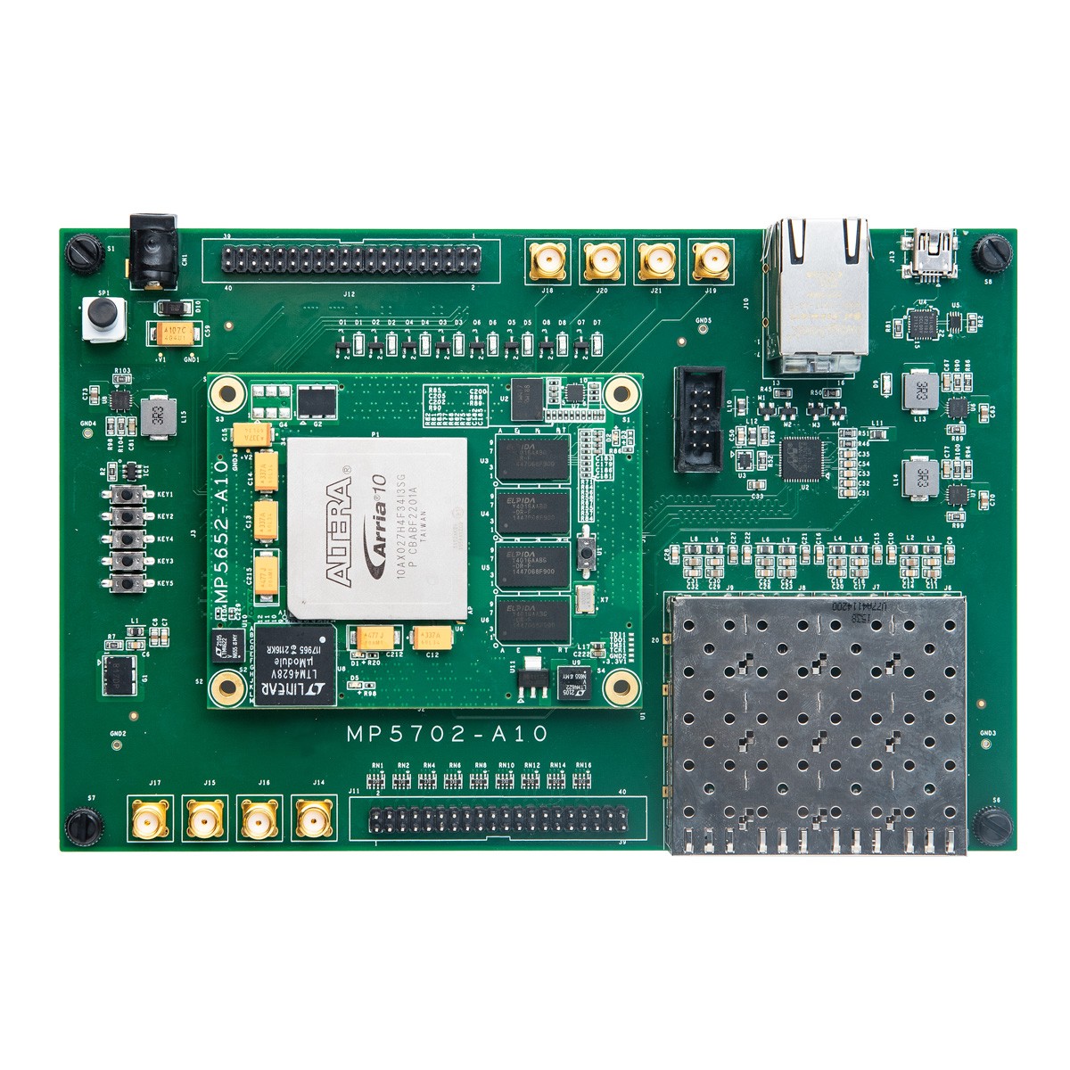
FPGA Intel Arria-10 GX series MP5652-A10
Key features of the Arria-10 GX series include:
- High-density and high-performance logic and DSP resources: The Arria-10 GX FPGAs offer a large number of logic elements (LEs) and digital signal processing (DSP) blocks. This allows for the implementation of complex algorithms and high-performance designs.
- High-speed transceivers: The Arria-10 GX series includes high-speed transceivers that support various protocols such as PCI Express (PCIe), Ethernet, and Interlaken. These transceivers can operate at data rates up to 28 Gbps, enabling high-speed data communication.
- High-speed memory interfaces: The Arria-10 GX FPGAs support various memory interfaces, including DDR4, DDR3, QDR IV, and RLDRAM 3. These interfaces provide high-bandwidth access to external memory devices.
- Integrated ARM Cortex-A9 processor: Some members of the Arria-10 GX series include an integrated dual-core ARM Cortex-A9 processor, which provides a powerful processing subsystem for embedded applications.
- System integration features: The Arria-10 GX FPGAs include various on-chip peripherals and interfaces, such as GPIO, I2C, SPI, UART, and JTAG, to facilitate system integration and communication with other components.
-

FPGA Xilinx K7 Kintex7 PCIe optical fiber communication
Here’s a general overview of the steps involved:
- Select an appropriate optical transceiver module: Depending on the specific requirements of your optical communication system, you would need to choose an optical transceiver module that supports the desired wavelength, data rate, and other characteristics. Common options include modules supporting Gigabit Ethernet (e.g., SFP/SFP+ modules) or higher-speed optical communication standards (e.g., QSFP/QSFP+ modules).
- Connect the optical transceiver to the FPGA: The FPGA typically interfaces with the optical transceiver module through high-speed serial links. The FPGA’s integrated transceivers or dedicated I/O pins designed for high-speed serial communication can be used for this purpose. You would need to follow the transceiver module’s datasheet and reference design guidelines to properly connect it to the FPGA.
- Implement the necessary protocols and signal processing: Once the physical connection is established, you would need to develop or configure the necessary protocols and signal processing algorithms for data transmission and reception. This can include implementing the necessary PCIe protocol for communication with the host system, as well as any additional signal processing algorithms required for encoding/decoding, modulation/demodulation, error correction, or other functions specific to your application.
- Integrate with PCIe interface: The Xilinx K7 Kintex7 FPGA has a built-in PCIe controller that allows it to communicate with the host system using the PCIe bus. You would need to configure and adapt the PCIe interface to meet the specific requirements of your optical communication system.
- Test and verify the communication: Once implemented, you would need to test and verify the optical fiber communication functionality using appropriate test equipment and methodologies. This can include verifying the data rate, bit error rate, and overall system performance.
-

FPGA XILINX-K7 KINTEX7 XC7K325 410T Industrial grade
Full model:FPGA XILINX-K7 KINTEX7 XC7K325 410T
- Series: Kintex-7: Xilinx’s Kintex-7 series FPGAs are designed for high-performance applications and offer a good balance between performance, power, and price.
- Device: XC7K325: This refers to the specific device within the Kintex-7 series. The XC7K325 is one of the variants available in this series, and it offers certain specifications, including logic cell capacity, DSP slices, and I/O count.
- Logic Capacity: The XC7K325 has a logic cell capacity of 325,000. Logic cells are programmable building blocks in an FPGA that can be configured to implement digital circuits and functions.
- DSP Slices: DSP slices are dedicated hardware resources within an FPGA that are optimized for digital signal processing tasks. The exact number of DSP slices in the XC7K325 may vary depending on the specific variant.
- I/O Count: The “410T” in the model number indicates that the XC7K325 has a total of 410 user I/O pins. These pins can be used to interface with external devices or other digital circuitry.
- Other Features: The XC7K325 FPGA may have other features, such as integrated memory blocks (BRAM), high-speed transceivers for data communication, and various configuration options.
-

Intelligent media motherboard robot motherboard subway screen main control board display motherboard
Some common features of intelligent media motherboards may include:
- High-speed data transfer: They often have support for the latest high-speed interfaces such as USB 3.0 or Thunderbolt, allowing for fast data transfer rates between external storage devices.
- Multiple expansion slots: These motherboards often have multiple PCIe slots to accommodate additional graphics cards, RAID controllers, or other expansion cards required for media-intensive tasks.
- Enhanced audio and video capabilities: Intelligent media motherboards may feature built-in high-definition audio codecs and dedicated video processing units for superior sound and video quality during media playback.
- Overclocking capabilities: They may have advanced overclocking features that allow users to push their hardware to higher frequencies, delivering enhanced performance for demanding media applications.
- Robust power delivery: Intelligent media motherboards typically have high-quality power delivery systems, including multiple power phases and robust voltage regulation, to ensure stable power supply to all components, even under heavy loads.
- Efficient cooling solutions: They often come with advanced cooling features such as larger heatsinks, additional fan headers, or liquid cooling support to keep the system temperature in check during extended media processing.
-
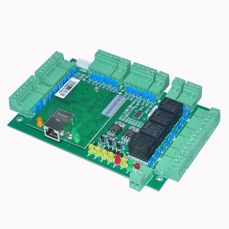
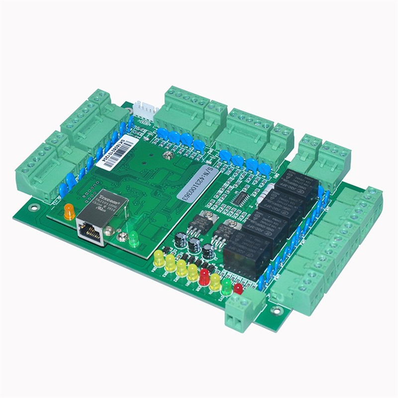
32 -bit ARM embedded industrial -grade access controller
◆ Environmental temperature: It is recommended to be within the range of -35 ℃ ~ 65 ℃
◆ Consumption: about 100mA (without load)
◆ Communication method: TCP/IP (default 100M)
◆ Number of user registration cards: 40,000
◆ Number of preservation records: 100,000
◆ The card reader input format: WG26 ~ 40 bit
◆ Controlled door output:Single door [1] Two doors [2] Four Dates [4]
◆ Number of card readers:Single door [1 pair] double door [2 pairs] four doors [4]
◆ Number of networking: unlimited
◆ Conventional function: time period/holiday/timing task, etc.
◆ Support time limit, the interval time setting of the card reading, etc.
◆ Support regional anti -submarine return, mutual lock, fire alarm alarm, etc.
◆ Embedded web server, you can visit the browser (B/S)
◆ Random distribution CD software, support the C/S architecture
◆ Support secondary development, DLL/message/mobile phone
◆ It can connect to the expansion board of the anti -theft fire alarm
◆ With V7.83 standard version of neutral software
◆ Size: 160mm long *106mm wide
-
Android board all -in -one motherboard self -service terminal motherboard
Google Android4.4 system. RK3288 is the world’s first quad-core ARM new A17 kernel chip in the world the first chip to support the latest super mali-T76X series GPU and the world’s first 4kx2k hard solution H.265 chip. It supports
-
32 -bit ARM embedded industrial -grade access controller
Environmental temperature:
It is recommended to be within the range of -35 ℃ ~ 65 ℃
-

Phone
-

E-mail
-

Whatsapp
-

Skype
-

Skype
-

Skype