Detailed PCBA production process (including the whole process of DIP), come in and see!
"Wave Soldering Process"
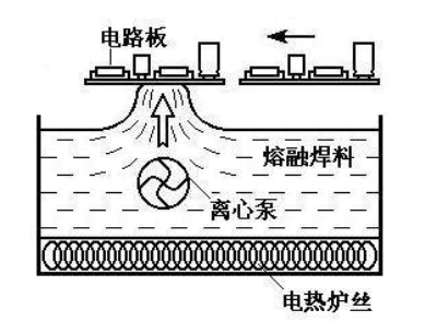
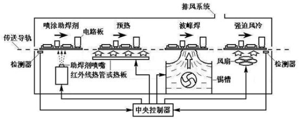
Wave soldering is generally a welding process for plug-in devices. It is a process in which the molten liquid solder, with the help of the pump, forms a specific shape of solder wave on the liquid surface of the solder tank, and the PCB of the inserted component passes through the solder wave peak at a specific Angle and a certain immersion depth on the transmission chain to achieve solder joint welding, as shown in the figure below.
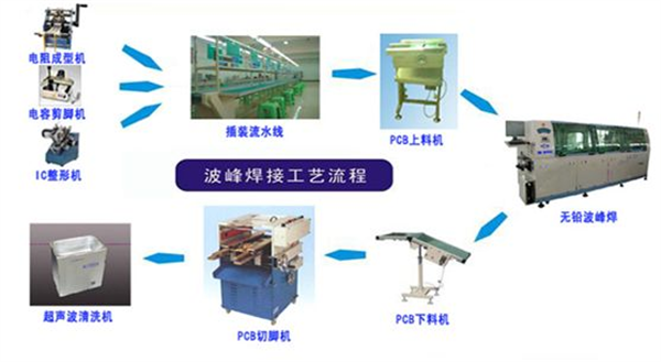
The general process flow is as follows: device insertion --PCB loading -- wave soldering --PCB unloading --DIP pin trimming -- cleaning, as shown in the figure below.
1.THC insertion technology
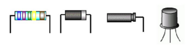
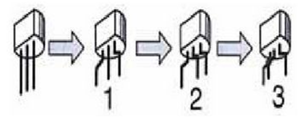
1. Component pin forming
DIP devices need to be shaped before insertion
(1)Hand-processed component shaping: The bent pin can be shaped with tweezers or a small screwdriver, as shown in the figure below.
(2) The machine processing of components shaping: the machine shaping of components is completed with a special shaping machinery, its working principle is that the feeder uses vibration feeding to feed materials, (such as plug-in transistor) with a divider to locate the transistor, the first step is to bend the pins on both sides of the left and right sides; The second step is to bend the middle pin back or forward to form. As shown in the following picture.
2. Insert components
Through hole insertion technology is divided into manual insertion and automatic mechanical equipment insertion
(1) Manual insertion and welding should first insert those components that need to be mechanically fixed, such as the cooling rack, bracket, clip, etc., of the power device, and then insert the components that need to be welded and fixed. Do not touch the component pins and copper foil on the printing plate directly when inserting.
(2) Mechanical automatic plug-in (referred to as AI) is the most advanced automated production technology in the installation of contemporary electronic products. The installation of automatic mechanical equipment should first insert those components with lower height, and then install those components with higher height. Valuable key components should be put into the final installation. The installation of heat dissipation rack, bracket, clip, etc. should be close to the welding process. The assembly sequence of PCB components is shown in the following figure.
3. Wave soldering
(1) Working principle of wave soldering
Wave soldering is a kind of technology that forms a specific shape of solder wave on the surface of molten liquid solder by means of pumping pressure, and forms a solder spot in the pin welding area when the assembly component inserted with the component passes through the solder wave at a fixed Angle. The component is first preheated in the welding machine preheating zone during the process of transmission by the chain conveyor (the component preheating and the temperature to be achieved are still controlled by the predetermined temperature curve). In actual welding, it is usually necessary to control the preheating temperature of the component surface, so many devices have added corresponding temperature detection devices (such as infrared detectors). After preheating, the assembly goes into the lead groove for welding. The tin tank contains molten liquid solder, and the nozzle at the bottom of the steel tank sprays a fixed shaped wave crest of the molten solder, so that when the welding surface of the component passes through the wave, it is heated by the solder wave, and the solder wave also moistens the welding area and expands to fill, finally achieving the welding process. Its working principle is shown in the figure below.
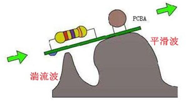
Wave soldering uses convection heat transfer principle to heat the welding area. The molten solder wave acts as a heat source, on the one hand flowing to wash the pin welding area, on the other hand also plays a heat conduction role, and the pin welding area is heated under this action. In order to ensure that the welding area heats up, the solder wave usually has a certain width, so that when the welding surface of the component passes through the wave, there is sufficient heating, wetting, and so on. In traditional wave soldering, single wave is generally used, and the wave is relatively flat. With the use of lead solder, it is currently adopted in the form of double wave. As shown in the following picture.
The pin of the component provides a way for the solder to dip into the metallized through hole in the solid state. When the pin touches the solder wave, the liquid solder climbs up the pin and hole wall by means of surface tension. The capillary action of metallized through holes improves the solder climbing. After the solder reaches the PcB pad, it spreads out under the action of the surface tension of the pad. The rising solder drains the flux gas and air from the through-hole, thus filling the through-hole and forming the solder joint after cooling.
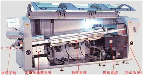
(2) The main components of the wave welding machine
A wave welding machine is mainly composed of a conveyor belt, a heater, a tin tank, a pump, and a flux foaming (or spray) device. It is mainly divided into flux adding zone, preheating zone, welding zone and cooling zone, as shown in the following figure.
3. Main differences between wave soldering and reflow welding
The main difference between wave soldering and reflow welding is that the heating source and solder supply method in the welding are different. In wave soldering, the solder is pre-heated and melted in the tank, and the solder wave produced by the pump plays the dual role of heat source and solder supply. The molten solder wave heats the through holes, pads, and component pins of the PCB, while also providing the solder needed to form solder joints. In reflow soldering, the solder (solder paste) is pre-allocated to the welding area of the PCB, and the role of the heat source during reflow is to re-melt the solder.
(1) 3 Introduction to selective wave soldering process
Wave soldering equipment has been invented for more than 50 years, and has the advantages of high production efficiency and large output in the manufacturing of through-hole components and circuit boards, so it was once the most important welding equipment in the automatic mass production of electronic products. However, there are some limitations in its application: (1) the welding parameters are different.
Different solder joints on the same circuit board may require very different welding parameters due to their different characteristics (such as heat capacity, pin spacing, tin penetration requirements, etc.). However, the characteristic of wave soldering is to complete the welding of all solder joints on the whole circuit board under the same set parameters, so different solder joints need to "settle" each other, which makes wave soldering more difficult to fully meet the welding requirements of high-quality circuit boards;
(2) High operating costs.
In the practical application of traditional wave soldering, the whole plate spraying of flux and the generation of tin slag bring high operating costs. Especially when lead-free welding, because the price of lead-free solder is more than 3 times that of lead solder, the increase in operating costs caused by tin slag is very surprising. In addition, the lead-free solder continues to melt the copper on the pad, and the composition of the solder in the tin cylinder will change over time, which requires regular addition of pure tin and expensive silver to solve;
(3) Maintenance and maintenance trouble.
The residual flux in the production will remain in the transmission system of wave soldering, and the tin slag generated needs to be removed regularly, which brings more complicated equipment maintenance and maintenance work to the user; For such reasons, selective wave soldering came into being.
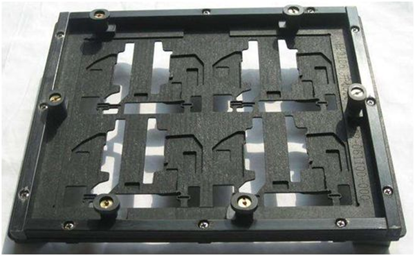
The so-called PCBA selective wave soldering still uses the original tin furnace, but the difference is that the board needs to be placed in the tin furnace carrier, which is what we often say about the furnace fixture, as shown in the figure below.
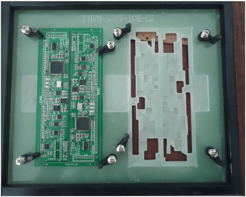
The parts requiring wave soldering are then exposed to the tin, and the other parts are protected with vehicle cladding, as shown below. This is a bit like putting on a life buoy in a swimming pool, the place covered by the life buoy will not get water, and replaced with a tin stove, the place covered by the vehicle will naturally not get tin, and there will be no problem of re-melting tin or falling parts.
"Through hole reflow Welding Process"
Through-hole reflow welding is a reflow welding process for inserting components, which is mainly used in the manufacture of surface assembly plates containing a few plug-ins. The core of the technology is the application method of solder paste.
1. Process introduction
According to the application method of solder paste, through hole reflow welding can be divided into three kinds: pipe printing through hole reflow welding process, solder paste printing through hole reflow welding process and molded tin sheet through hole reflow welding process.
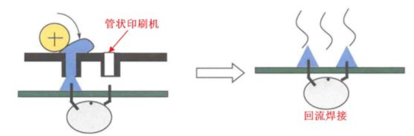
1) Tubular printing through hole reflow welding process
Tubular printing through hole reflow welding process is the earliest application of through hole components reflow welding process, which is mainly used in the manufacture of color TV tuner. The core of the process is the solder paste tubular press, the process is shown in the figure below.
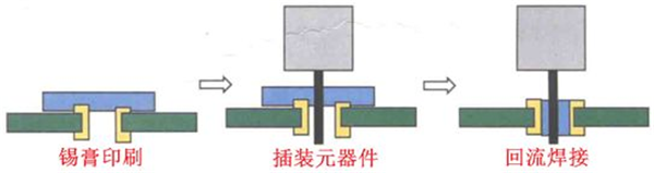
2) Solder paste printing through hole reflow welding process
Solder paste printing through hole reflow welding process is currently the most widely used through hole reflow welding process, mainly used for mixed PCBA containing a small number of plug-ins, the process is fully compatible with conventional reflow welding process, no special process equipment is required, the only requirement is that the welded plug-in components must be suitable for through hole reflow welding, the process is shown in the following figure.
3) Molding tin sheet through hole reflow welding process
Molded tin sheet through hole reflow welding process is mainly used for multi-pin connectors, solder is not solder paste but molded tin sheet, generally by the connector manufacturer directly added, assembly can only be heated.
Through hole reflow design requirements
1.PCB design requirements
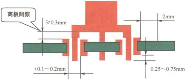
(1) Suitable for PCB thickness less than or equal to 1.6mm board.
(2) The minimum width of the pad is 0.25mm, and the molten solder paste is "pulled" once, and the tin bead is not formed.
(3) The component off-board gap (Stand-off) should be greater than 0.3mm
(4) The appropriate length of the lead sticking out of the pad is 0.25~0.75mm.
(5) The minimum distance between fine spacing components such as 0603 and the pad is 2mm.
(6) The maximum opening of the steel mesh can be expanded by 1.5mm.
(7)The aperture is the lead diameter plus 0.1~0.2mm. As shown in the following picture.
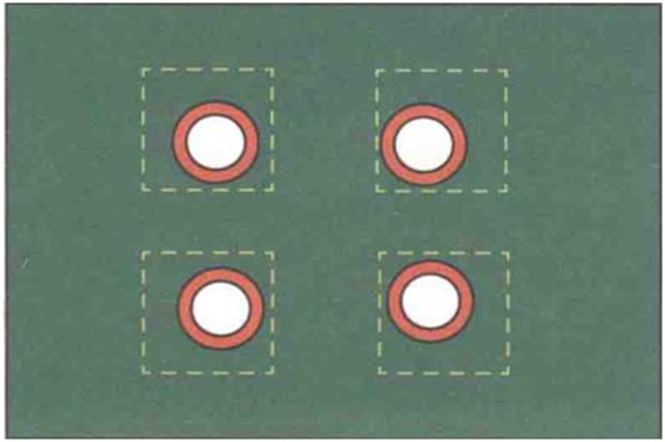
"Steel mesh window opening requirements"
In general, in order to achieve 50% hole filling, the steel mesh window must be expanded, the specific amount of external expansion should be determined according to the PCB thickness, the thickness of the steel mesh, the gap between the hole and the lead and other factors.
In general, as long as the expansion does not exceed 2mm, the solder paste will be pulled back and filled into the hole. It should be noted that the external expansion can not be compressed by the component package, or must avoid the package body of the component, and form a tin bead on one side, as shown in the following figure.
"Introduction to the conventional Assembly Process of PCBA"
1) Single-side mounting
The process flow is shown in the figure below
2) Single side insertion
The process flow is shown in Figure 5 below
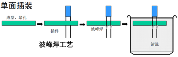
The forming of the device pins in wave soldering is one of the least efficient parts of the production process, which correspondingly brings the risk of electrostatic damage and prolongs the delivery time, and also increases the chance of error.
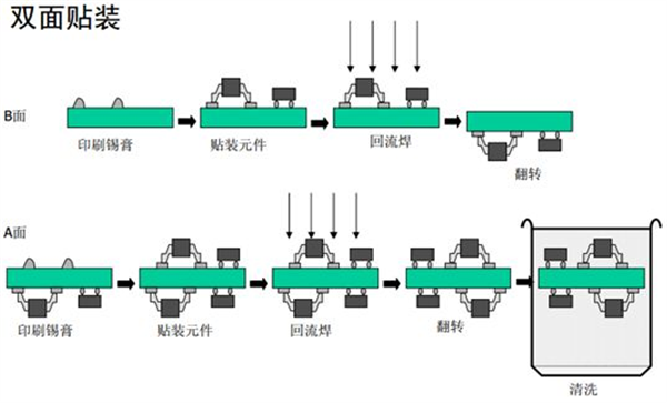
3) Double-sided mounting
The process flow is shown in the figure below
4) One side mixed
The process flow is shown in the figure below
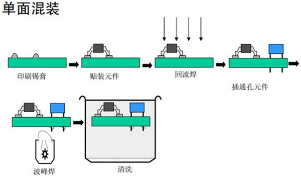
If there are few through-hole components, reflow welding and manual welding can be used.
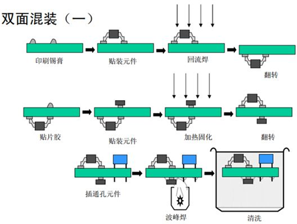
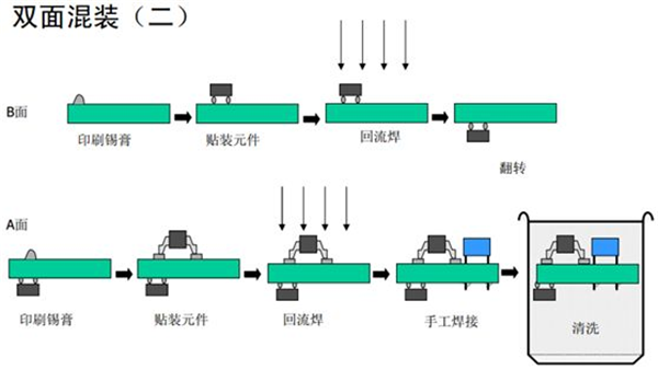
5) Double-sided mixing
The process flow is shown in the figure below
If there are more double-sided SMD devices and few THT components, the plug-in devices can be reflow or manual welding. The process flow chart is shown below.