One-stop Electronic Manufacturing Services, help you easily achieve your electronic products from PCB & PCBA


FPGA Xilinx K7 Kintex7 PCIe optical fiber communication
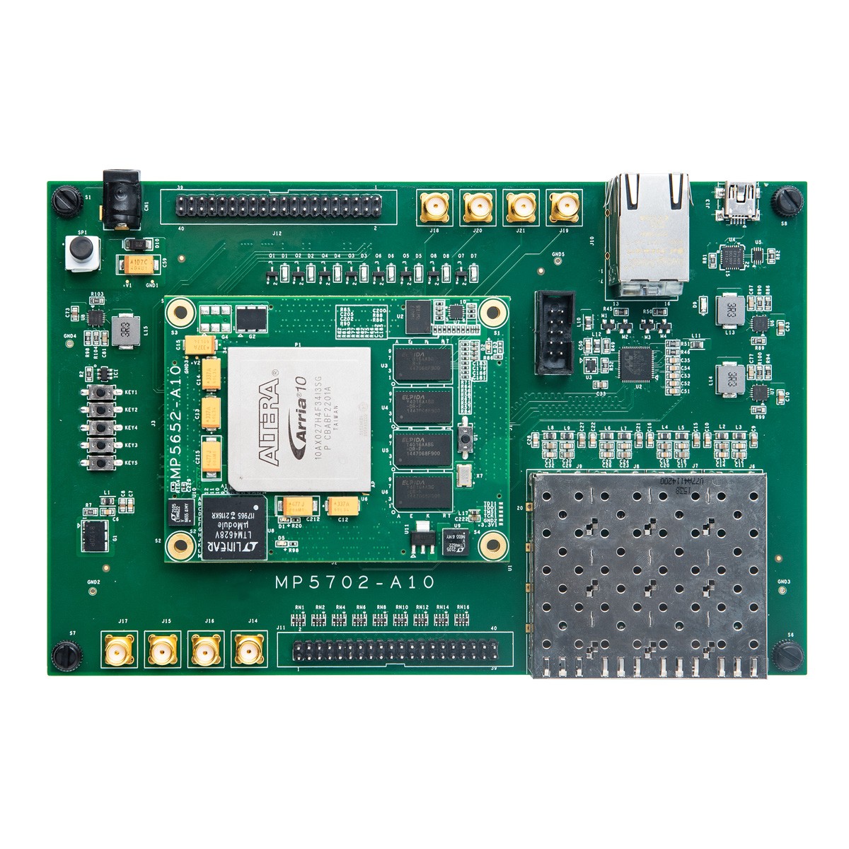
- DDR3 SDRAM: 16GB DDR3 64bit bus, data rate 1600Mbps
- QSPI Flash: A piece of 128mbit QSPIFLASH, which can be used for FPGA configuration files and user data storage
- PCLEX8 interface: The standard PCLEX8 interface is used to communicate with the PCIE communication of the computer motherboard. It supports the PCI, Express 2.0 standard. The single -channel communication rate can be as high as 5Gbps
- USB UART serial port: A serial port, connect to the PC through the miniusb cable to perform serial communication
- Micro SD card: Microsd card seat all the way, you can connect the standard Microsd card
- Temperature sensor: a temperature sensor chip LM75, which can monitor the environmental temperature around the development board
- FMC extension port: a FMC HPC and a FMCLPC, which can be compatible with various standard expansion board cards
- ERF8 high -speed connection terminal: 2 ERF8 ports, which supports ultra -high -speed signal transmission 40pin extension: reserved a general extension IO interface with 2.54mm40pin, effective O has 17 pairs, support 3.3V
- The peripheral connection of the level and the 5V level can connect the peripheral peripherals of different general -purpose 1O interfaces
- SMA terminal; 13 high -quality gold -plated SMA heads, which is convenient for users to cooperate with high -speed AD/DA FMC expansion cards for signal collection and processing
- Clock Management: Multi -clock source. These include the 200MHz system differential clock source SIT9102
- Differential crystal oscillating: 50MHz crystal and SI5338P programmable clock management chip: also equipped with
- 66MHz EMCCLK. Can accurately adapt to different use clock frequency
- JTAG port: 10 stitches 2.54mm standard JTAG port, for download and debugging of FPGA programs
- Sub -reset voltage monitoring chip: a piece of ADM706R voltage monitoring chip, and the button with the button provides a global reset signal for the system
- LED: 11 LED lights, indicate the power supply of the board card, config_done signal, FMC
- Power indicator signal, and 4 user LED
- Key and switch: 6 keys and 4 switches are FPGA reset buttons,
- Program B button and 4 user keys are composed. 4 single -knife double throw switch
Write your message here and send it to us
Products categories


-

Phone
-

E-mail
-

Whatsapp
-

Skype
-

Skype
-

Skype