
High precision PCBA circuit board DIP plug-in selective wave soldering welding design should follow the requirements!
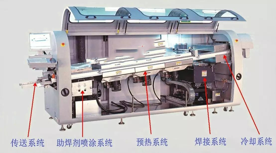
In the traditional electronic assembly process, wave welding technology is generally used for the welding of printed board components with perforated insert elements (PTH).
DIP wave soldering has many disadvantages:
1. High-density, fine-pitch SMD components cannot be distributed on the welding surface;
2. There are many bridging and missing soldering;
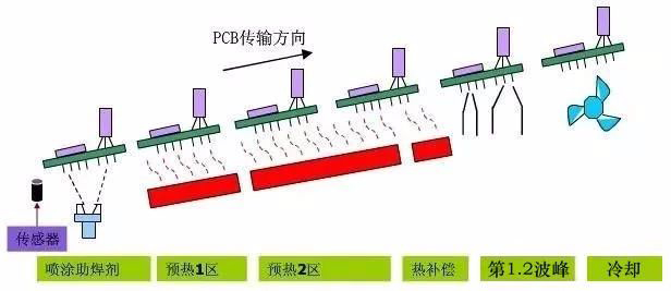
3.Flux needs to be sprayed; the printed board is warped and deformed by a large thermal shock.
As the current circuit assembly density is getting higher and higher, it is inevitable that high-density, fine-pitch SMD components will be distributed on the soldering surface. The traditional wave soldering process has been powerless to do this. Generally, the SMD components on the soldering surface can only be reflow soldered separately. , and then manually repair the remaining plug-in solder joints, but there is a problem of poor solder joint quality consistency.
As the soldering of through-hole components (especially large-capacity or fine-pitch components) becomes more and more difficult, especially for products with lead-free and high reliability requirements, the soldering quality of manual soldering can no longer meet high-quality electrical equipment. According to the requirements of production, wave soldering cannot fully meet the production and application of small batches and multiple varieties in specific use. The application of selective wave soldering has developed rapidly in recent years.
For PCBA circuit boards with only THT perforated components, because wave soldering technology is still the most effective processing method at present, it is not necessary to replace wave soldering with selective soldering, which is very important. However, selective soldering is essential for mixed technology boards and, depending on the type of nozzle used, wave soldering techniques can be replicated in an elegant manner.
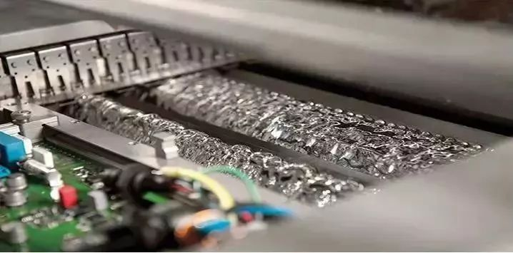
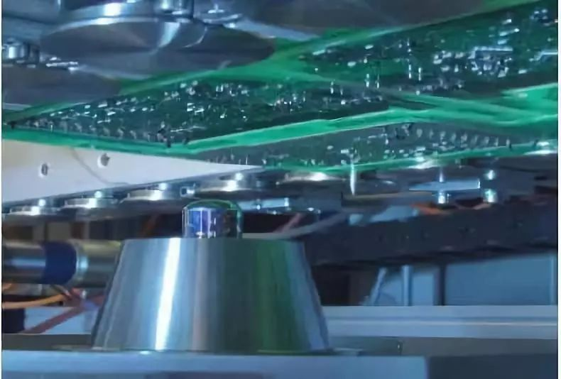
There are two different processes for selective soldering: drag soldering and dip soldering.
The selective drag soldering process is done on a single small tip solder wave. The drag soldering process is suitable for soldering on very tight spaces on the PCB. For example: individual solder joints or pins, a single row of pins can be dragged and soldered.
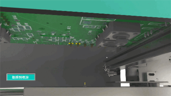
Selective wave soldering technology is a newly developed technology in SMT technology, and its appearance largely meets the assembly requirements of high-density and diverse mixed PCB boards. Selective wave soldering has the advantages of independent setting of solder joint parameters, less thermal shock to PCB, less flux spraying, and strong soldering reliability. It is gradually becoming an indispensable soldering technology for complex PCBs.
As we all know, the PCBA circuit board design stage determines 80% of the manufacturing cost of the product. Likewise, many quality characteristics are fixed at design time. Therefore, it is very important to fully consider manufacturing factors in the PCB circuit board design process.
A good DFM is an important way for PCBA mounting component manufacturers to reduce manufacturing defects, simplify the manufacturing process, shorten the manufacturing cycle, reduce manufacturing costs, optimize quality control, enhance product market competitiveness, and improve product reliability and durability. It can enable enterprises to obtain the best benefits with the least investment and achieve twice the result with half the effort.
The development of surface mount components to today requires SMT engineers not only to be proficient in circuit board design technology, but also to have an in-depth understanding and rich practical experience in SMT technology. Because a designer who does not understand the flow characteristics of solder paste and solder is often difficult to understand the reasons and principles of bridging, tipping, tombstone, wicking, etc., and it is difficult to work hard to design the pad pattern reasonably. It is difficult to deal with various design issues from the perspectives of design manufacturability, testability, and cost and expense reduction. A perfectly designed solution will cost a lot of manufacturing and testing costs if the DFM and DFT (design for detectability) are poor.


