
SMT uses conventional solder paste air reflow welding cavity analysis and solution (2023 Essence Edition), you deserve it!
1 Introduction
In the circuit board assembly, solder paste is printed on the circuit board solder pad first, and then various electronic components are affixed. Finally, after the reflow furnace, the tin beads in the solder paste are melted and all kinds of electronic components and the solder pad of the circuit board are welded together to realize the assembly of electrical submodules. surfacemounttechnology (sMT) is increasingly used in high-density packaging products, such as system level package (siP), ballgridarray (BGA) devices, and power bare Chip, square flat pin-less package (quad aatNo-lead, referred to as QFN) device.
Due to the characteristics of solder paste welding process and materials, after reflow welding of these large solder surface devices, there will be holes in the solder welding area, which will affect the electrical properties, thermal properties and mechanical properties of the product Performance, and even lead to product failure, therefore, to improve the solder paste reflow welding cavity has become a process and technical problem that must be solved, some researchers have analyzed and studied the causes of BGA solder ball welding cavity, and provided improvement solutions, conventional solder paste reflow welding process welding area of QFN greater than 10mm2 or welding area greater than 6 mm2's bare chip solution is lacking.
Use Preformsolder welding and vacuum reflux furnace welding to improve the weld hole. Prefabricated solder requires special equipment to point flux. For example, the chip is offset and tilted seriously after the chip is placed directly on the prefabricated solder. If the flux mount chip is reflow and then point, the process is increased by two reflow, and the cost of prefabricated solder and flux material is much higher than the solder paste.
Vacuum reflux equipment is more expensive, the vacuum capacity of the independent vacuum chamber is very low, the cost performance is not high, and the tin splashing problem is serious, which is an important factor in the application of high-density and small-pitch products. In this paper, based on the conventional solder paste reflow welding process, a new secondary reflow welding process is developed and introduced to improve the welding cavity and solve the problems of bonding and plastic seal cracking caused by welding cavity.
2 Solder paste printing reflow welding cavity and production mechanism
2.1 Welding cavity
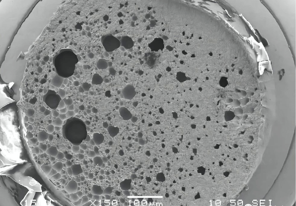
After reflow welding, the product was tested under x-ray. The holes in the welding zone with lighter color were found to be due to insufficient solder in the welding layer, as shown in Figure 1
X-ray detection of the bubble hole
2.2 Formation mechanism of welding cavity
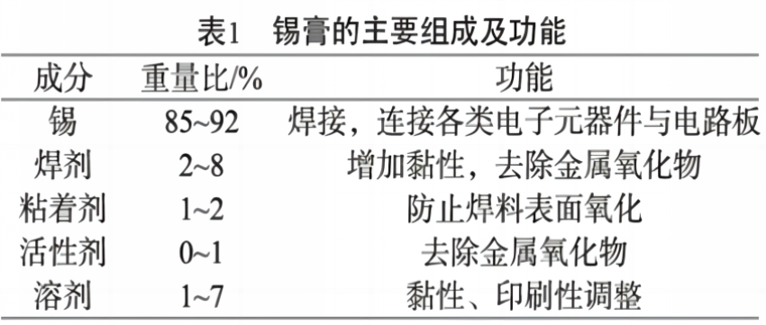
Taking sAC305 solder paste as an example, the main composition and function are shown in Table 1. The flux and tin beads are bonded together in paste shape. The weight ratio of tin solder to flux is about 9:1, and the volume ratio is about 1:1.
After the solder paste is printed and mounted with various electronic components, the solder paste will undergo four stages of preheating, activation, reflux and cooling when it passes through the reflux furnace. The state of the solder paste is also different with different temperatures in different stages, as shown in Figure 2.
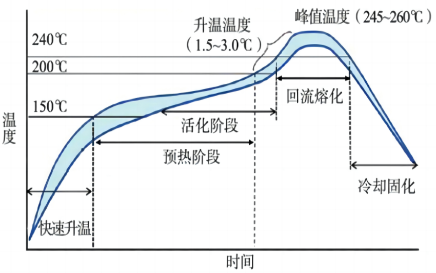
Profile reference for each area of reflow soldering
In the preheating and activation stage, the volatile components in the flux in the solder paste will be volatilized into gas when heated. At the same time, gases will be produced when the oxide on the surface of the welding layer is removed. Some of these gases will volatilize and leave the solder paste, and the solder beads will be tightly condensed due to the volatilization of flux. In the reflux stage, the remaining flux in the solder paste will evaporate quickly, the tin beads will melt, a small amount of flux volatile gas and most of the air between the tin beads will not be dispersed in time, and the residual in the molten tin and under the tension of the molten tin are hamburger sandwich structure and are caught by the circuit board solder pad and electronic components, and the gas wrapped in the liquid tin is difficult to escape only by the upward buoyancy The upper melting time is very short. When the molten tin cools down and becomes solid tin, pores appear in the welding layer and solder holes are formed, as shown in Figure 3.
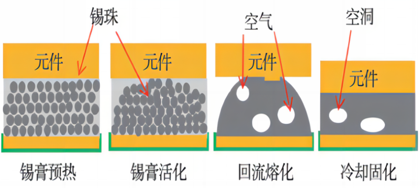
Schematic diagram of void generated by solder paste reflow welding
The root cause of welding cavity is that the air or volatile gas wrapped in the solder paste after melting is not completely discharged. The influencing factors include solder paste material, solder paste printing shape, solder paste printing amount, reflux temperature, reflux time, welding size, structure and so on.
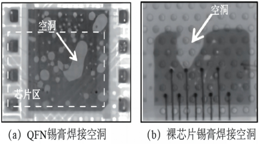
3. Verification of influencing factors of solder paste printing reflow welding holes
QFN and bare chip tests were used to confirm the main causes of reflow welding voids, and to find ways to improve the reflow welding voids printed by solder paste. QFN and bare chip solder paste reflow welding product profile is shown in Figure 4,QFN welding surface size is 4.4mmx4.1mm, welding surface is tinned layer (100% pure tin); The welding size of the bare chip is 3.0mmx2.3mm, the welding layer is sputtered nickel-vanadium bimetallic layer, and the surface layer is vanadium. The welding pad of the substrate was electroless nickel-palladium gold-dipping, and the thickness was 0.4μm/0.06μm/0.04μm. SAC305 solder paste is used, the solder paste printing equipment is DEK Horizon APix, the reflux furnace equipment is BTUPyramax150N, and the x-ray equipment is DAGExD7500VR.
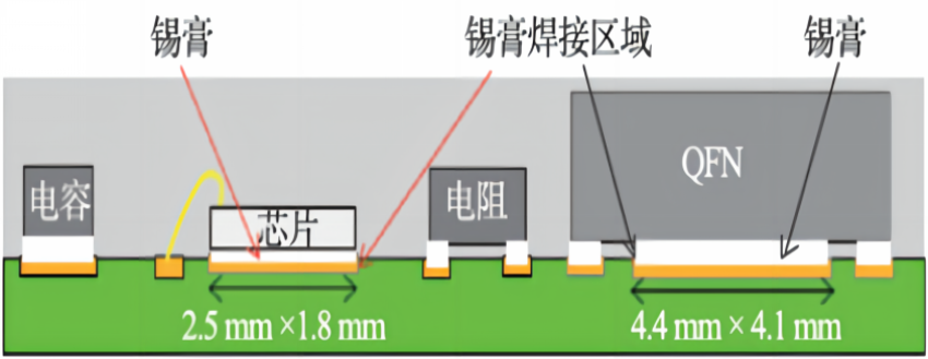
QFN and bare chip welding drawings
To facilitate comparison of test results, reflow welding was performed under the conditions in Table 2.
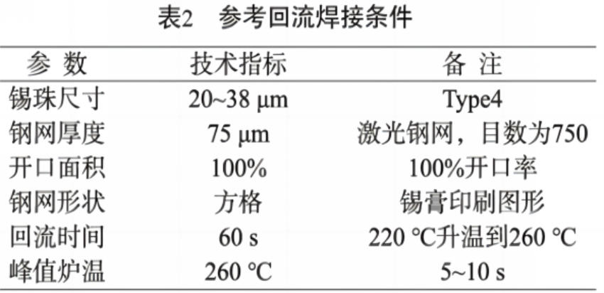
Reflow welding condition table
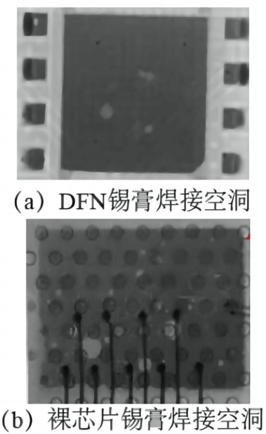
After surface mounting and reflow welding were completed, the welding layer was detected by X-ray, and it was found that there were large holes in the welding layer at the bottom of QFN and bare chip, as shown in Figure 5.
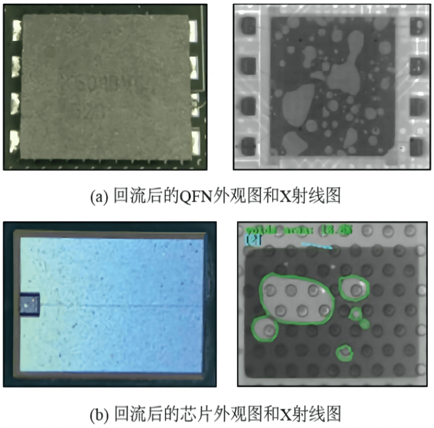
QFN and Chip Hologram (X-ray)
Since tin bead size, steel mesh thickness, opening area rate, steel mesh shape, reflux time and peak furnace temperature will all affect reflow welding voids, there are many influencing factors, which will be directly verified by DOE test, and the number of experimental groups will be too large. It is necessary to quickly screen and determine the main influencing factors through correlation comparison test, and then further optimize the main influencing factors through DOE.
3.1 Dimensions of solder holes and solder paste tin beads
With type3 (bead size 25-45 μm)SAC305 solder paste test, other conditions remain unchanged. After reflow, the holes in the solder layer are measured and compared with type4 solder paste. It is found that the holes in the solder layer are not significantly different between the two kinds of solder paste, indicating that the solder paste with different bead size has no obvious influence on the holes in the solder layer, which is not an influencing factor, as shown in FIG. 6 As shown.
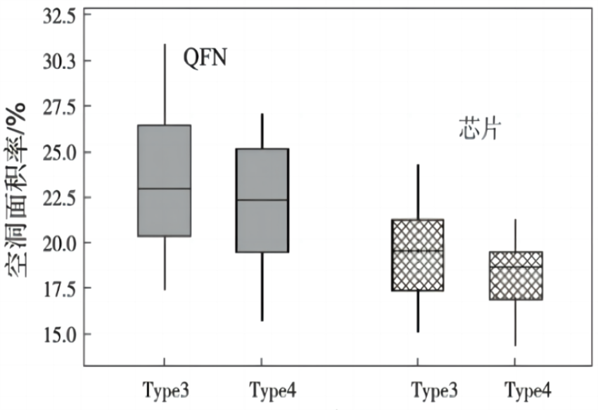
Comparison of metallic tin powder holes with different particle sizes
3.2 Thickness of welding cavity and printed steel mesh
After reflow, the cavity area of the welded layer was measured with the printed steel mesh with the thickness of 50 μm, 100 μm and 125 μm, and other conditions remained unchanged. It was found that the effect of different thickness of steel mesh (solder paste) on QFN was compared with that of the printed steel mesh with the thickness of 75 μm As the thickness of the steel mesh increases, the cavity area gradually decreases slowly. After reaching a certain thickness (100μm), the cavity area will reverse and begin to increase with the increase of the thickness of the steel mesh, as shown in Figure 7.
This shows that when the amount of solder paste is increased, the liquid tin with reflux is covered by the chip, and the outlet of residual air escape is only narrow on four sides. When the amount of solder paste is changed, the outlet of residual air escape is also increased, and the instant burst of air wrapped in liquid tin or volatile gas escaping liquid tin will cause liquid tin to splash around QFN and the chip.
The test found that with the increase of the thickness of the steel mesh, the bubble burst caused by the escape of air or volatile gas will also increase, and the probability of tin splashing around QFN and chip will also increase correspondingly.
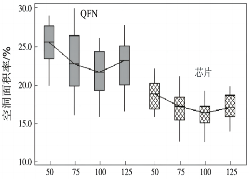
Comparison of holes in steel mesh of different thickness
3.3 Area ratio of welding cavity and steel mesh opening
The printed steel mesh with the opening rate of 100%, 90% and 80% was tested, and other conditions remained unchanged. After reflow, the cavity area of the welded layer was measured and compared with the printed steel mesh with the 100% opening rate. It was found that there was no significant difference in the cavity of the welded layer under the conditions of the opening rate of 100% and 90% 80%, as shown in Figure 8.
Cavity comparison of different opening area of different steel mesh
3.4 Welded cavity and printed steel mesh shape
With the printing shape test of the solder paste of strip b and inclined grid c, other conditions remain unchanged. After reflow, the cavity area of the welding layer is measured and compared with the printing shape of grid a. It is found that there is no significant difference in the cavity of the welding layer under the conditions of grid, strip and inclined grid, as shown in Figure 9.
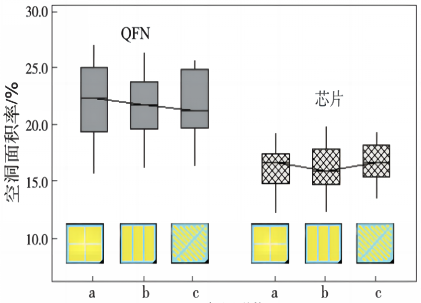
Comparison of holes in different opening modes of steel mesh
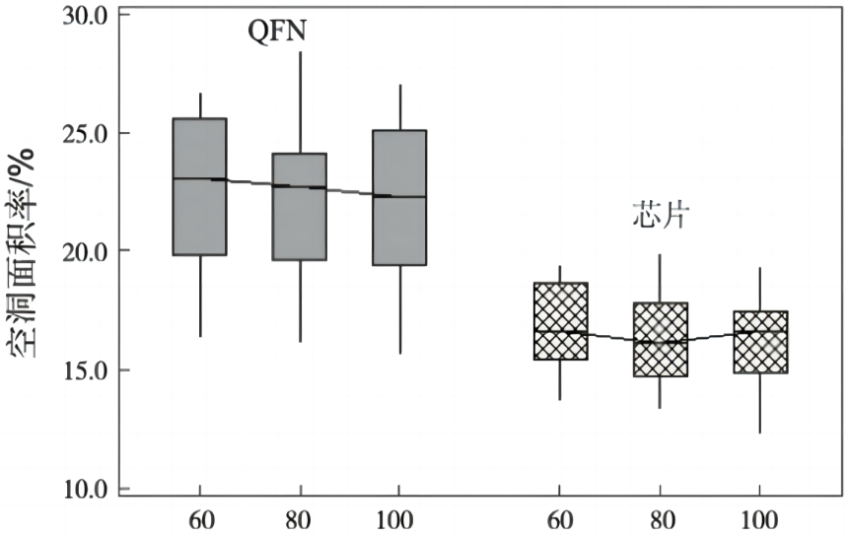
3.5 Welding cavity and reflux time
After prolonged reflux time (70 s, 80 s, 90 s) test, other conditions remain unchanged, the hole in the welding layer was measured after reflux, and compared with the reflux time of 60 s, it was found that with the increase of reflux time, the welding hole area decreased, but the reduction amplitude gradually decreased with the increase of time, as shown in Figure 10. This shows that in the case of insufficient reflux time, increasing the reflux time is conducive to the full overflow of air wrapped in molten liquid tin, but after the reflux time increases to a certain time, the air wrapped in liquid tin is difficult to overflow again. Reflux time is one of the factors affecting the welding cavity.
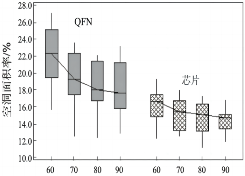
Void comparison of different reflux time lengths
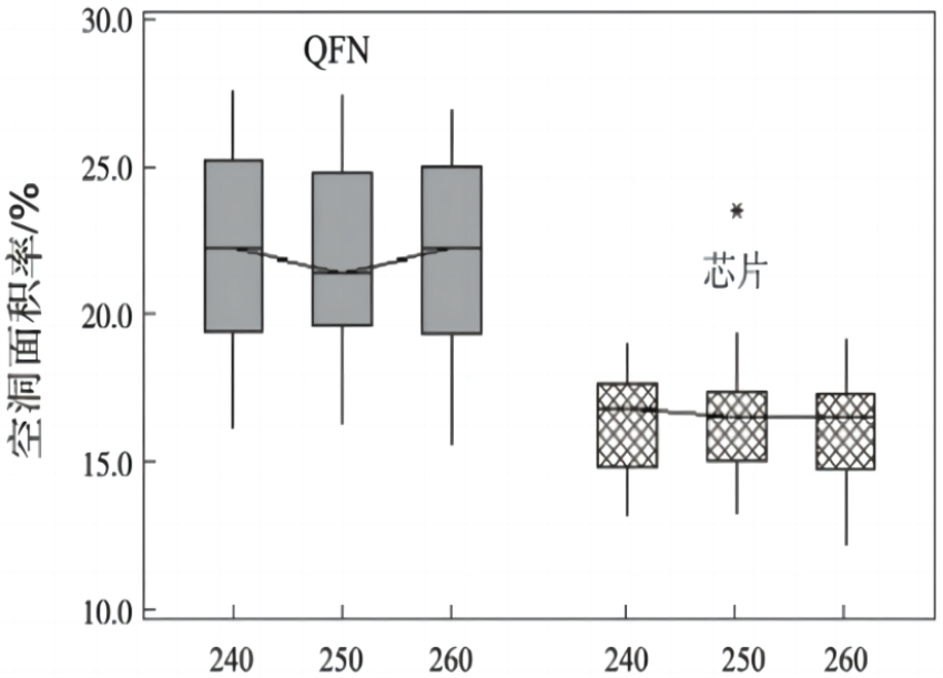
3.6 Welding cavity and peak furnace temperature
With 240 ℃ and 250 ℃ peak furnace temperature test and other conditions unchanged, the cavity area of the welded layer was measured after reflow, and compared with 260 ℃ peak furnace temperature, it was found that under different peak furnace temperature conditions, the cavity of the welded layer of QFN and chip did not change significantly, as shown in Figure 11. It shows that different peak furnace temperature has no obvious effect on QFN and the hole in the welding layer of the chip, which is not an influencing factor.
Void comparison of different peak temperatures
The above tests indicate that the significant factors affecting the weld layer cavity of QFN and chip are reflux time and steel mesh thickness.
4 Solder paste printing reflow welding cavity improvement
4.1DOE test to improve welding cavity
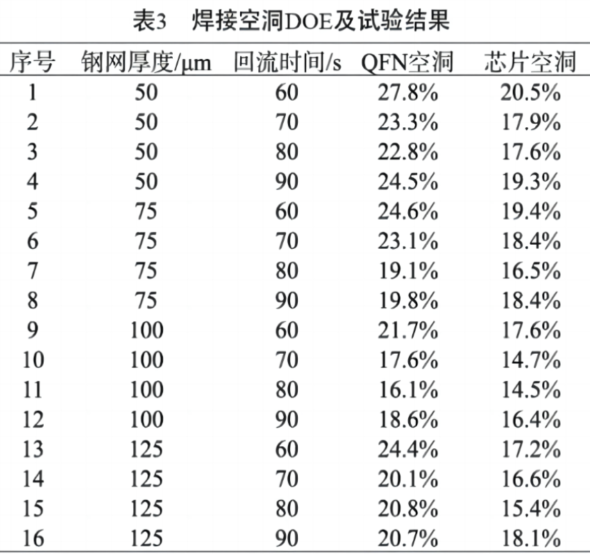
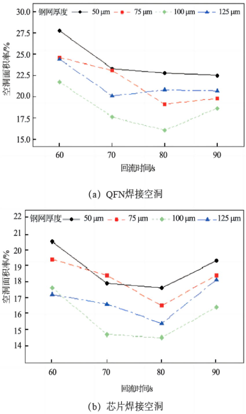
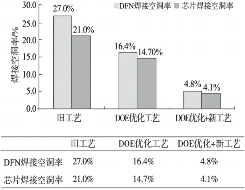
The hole in the welding layer of QFN and chip was improved by finding the optimal value of the main influencing factors (reflux time and steel mesh thickness). The solder paste was SAC305 type4, the steel mesh shape was grid type (100% opening degree), the peak furnace temperature was 260 ℃, and other test conditions were the same as those of the test equipment. DOE test and results were shown in Table 3. The influences of steel mesh thickness and reflux time on QFN and chip welding holes are shown in Figure 12. Through the interaction analysis of main influencing factors, It is found that using 100 μm steel mesh thickness and 80 s reflux time can significantly reduce the welding cavity of QFN and chip. The welding cavity rate of QFN is reduced from the maximum 27.8% to 16.1%, and the welding cavity rate of chip is reduced from the maximum 20.5% to 14.5%.
In the test, 1000 products were produced under the optimal conditions (100 μm steel mesh thickness, 80 s reflux time), and the welding cavity rate of 100 QFN and chip was randomly measured. The average welding cavity rate of QFN was 16.4%, and the average welding cavity rate of chip was 14.7% The weld cavity rate of the chip and the chip are obviously reduced.
4.2 The new process improves the welding cavity
The actual production situation and test show that when the welding cavity area at the bottom of the chip is less than 10%, the chip cavity position cracking problem will not occur during the lead bonding and molding. The process parameters optimized by DOE cannot meet the requirements of analyzing and solving the holes in the conventional solder paste reflow welding, and the welding cavity area rate of the chip needs to be further reduced.
Since the chip covered on the solder prevents the gas in the solder from escaping, the hole rate at the bottom of the chip is further reduced by eliminating or reducing the solder coated gas. A new process of reflow welding with two solder paste printing is adopted: one solder paste printing, one reflow not covering QFN and bare chip discharging the gas in solder; The specific process of secondary solder paste printing, patch and secondary reflux is shown in Figure 13.
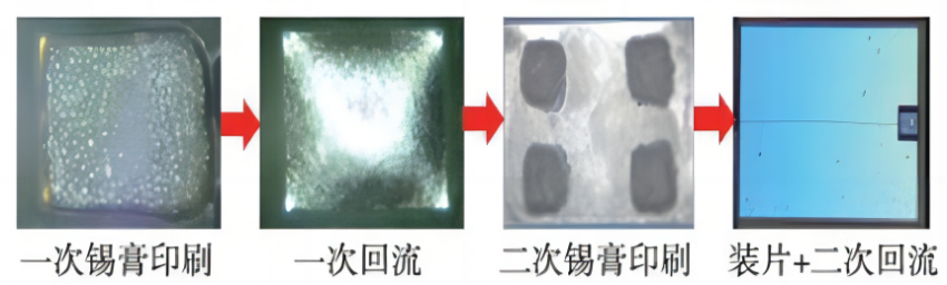
When the 75μm thick solder paste is printed for the first time, most of the gas in the solder without chip cover escapes from the surface, and the thickness after reflux is about 50μm. After the completion of the primary reflux, small squares are printed on the surface of the cooled solidified solder (in order to reduce the amount of solder paste, reduce the amount of gas spillover, reduce or eliminate solder spatter), and the solder paste with a thickness of 50 μm (the above test results show that 100 μm is the best, so the thickness of the secondary printing is 100 μm.50 μm=50 μm), then install the chip, and then return through 80 s. There is almost no hole in the solder after the first printing and reflow, and the solder paste in the second printing is small, and the welding hole is small, as shown in Figure 14.
After two printings of solder paste, hollow drawing
4.3 Verification of welding cavity effect
Production of 2000 products (the thickness of the first printing steel mesh is 75 μm, the thickness of the second printing steel mesh is 50 μm), other conditions unchanged, random measurement of 500 QFN and chip welding cavity rate, found that the new process after the first reflux no cavity, after the second reflux QFN The maximum welding cavity rate is 4.8%, and the maximum welding cavity rate of the chip is 4.1%. Compared with the original single-paste printing welding process and the DOE optimized process, the welding cavity is significantly reduced, as shown in Figure 15. No chip cracks were found after functional tests of all products.
5 Summary
The optimization of solder paste printing amount and reflux time can reduce the welding cavity area, but the welding cavity rate is still large. Using two solder paste printing reflow welding techniques can effectively and maximize the welding cavity rate. The welding area of QFN circuit bare chip can be 4.4mm x4.1mm and 3.0mm x2.3mm respectively in mass production The cavity rate of reflow welding is controlled below 5%, which improves the quality and reliability of reflow welding. The research in this paper provides an important reference for improving the welding cavity problem of large area welding surface.


