


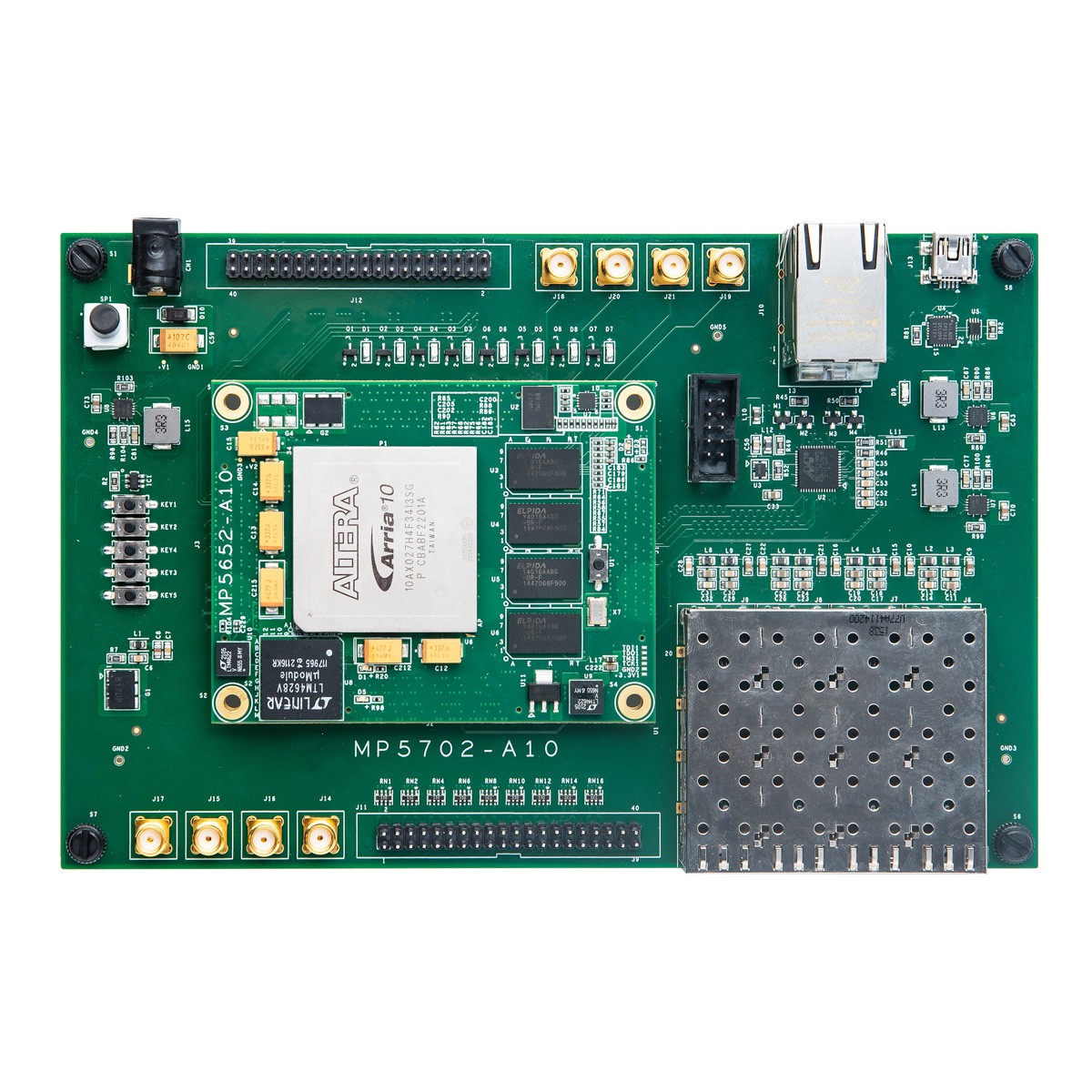
FPGA XILINX-K7 KINTEX7 XC7K325 410T Industrial grade
DDR3 SDRAMQ: 16GB DDR3, 4GB per piece, 16bit Data Bit Data Bid SPI Flash: One piece of 128MBITQSPIFLASH, which can be used for FPGA configuration files and user data storage FPGA Bank interface levels: adjustable 1.8V, 2.5V, 3.3V electrical If you need to replace the level, you only need to replace the corresponding position of the magnetic bead to achieve adjustment. Core board power supply: 5V-12V range of power supply EEPROM; M24C02-WMN6TP is based on I2C bus device. Following the starting method of the core board of the second-line protocol: supports two start-up modes, which are JTAG, QSPI Flash connectors. Extended port, 120pin, Panasonic AXK5A2137yg MP5700 bottom plate SFP interface: 2 optical modules can achieve high -speed optical fiber communication, as high as 6GB/s bottom plate clock: 1 200MHz reference clock connected to the core board MRCC clock tube foot, 1 125MHz The GTX clock tube feet bottom plate of the clock connect to the core board is 40 -pin expansion port: reserve a 2.54mm standard spacing 40 -shot extension port, which is used to connect the customer’s own design module. Essence Core board clock: there are multiple clock sources on the board. These include the 200MHz system clock, the 125MHz GTX clock, and the 66MHz EMCCLK clock. JTAG port: 10 stitches 2.54mm standard JTAG port, for downloading and debugging LEDs for FPGA programs: a total of 6 red LED lights in the core board, indicating the power supply of the board card, 4 signal indicator lights and FPGA IO tube feet directly connected directly Key: 4 keys. 4 keys. They are FPGA reset buttons, Program_b keys and two user keys.
The FPGA Xilinx-K7 Kintex7 XC7K325 410T is a specific model of FPGA (Field-Programmable Gate Array) developed by Xilinx. Here are some key details about this FPGA:Series: Kintex-7: Xilinx’s Kintex-7 series FPGAs are designed for high-performance applications and offer a good balance between performance, power, and price.Device: XC7K325: This refers to the specific device within the Kintex-7 series. The XC7K325 is one of the variants available in this series, and it offers certain specifications, including logic cell capacity, DSP slices, and I/O count.Logic Capacity: The XC7K325 has a logic cell capacity of 325,000. Logic cells are programmable building blocks in an FPGA that can be configured to implement digital circuits and functions.DSP Slices: DSP slices are dedicated hardware resources within an FPGA that are optimized for digital signal processing tasks. The exact number of DSP slices in the XC7K325 may vary depending on the specific variant.I/O Count: The “410T” in the model number indicates that the XC7K325 has a total of 410 user I/O pins. These pins can be used to interface with external devices or other digital circuitry.Other Features: The XC7K325 FPGA may have other features, such as integrated memory blocks (BRAM), high-speed transceivers for data communication, and various configuration options.It’s important to note that FPGAs like the Xilinx-K7 Kintex7 XC7K325 are programmable devices that allow you to implement custom digital circuits and functionalities by programming their logic cells. This flexibility makes them suitable for a wide range of applications, including high-performance computing, digital signal processing, and hardware acceleration.
Products categories


-

Phone
-

E-mail
-

Whatsapp
-

Skype
-

Skype
-

Skype