


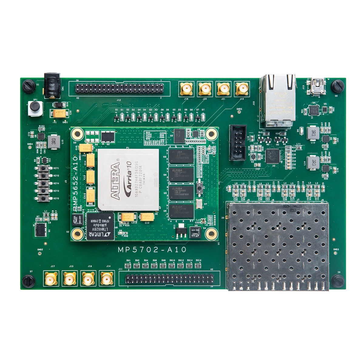
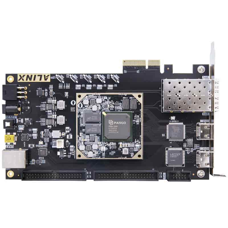
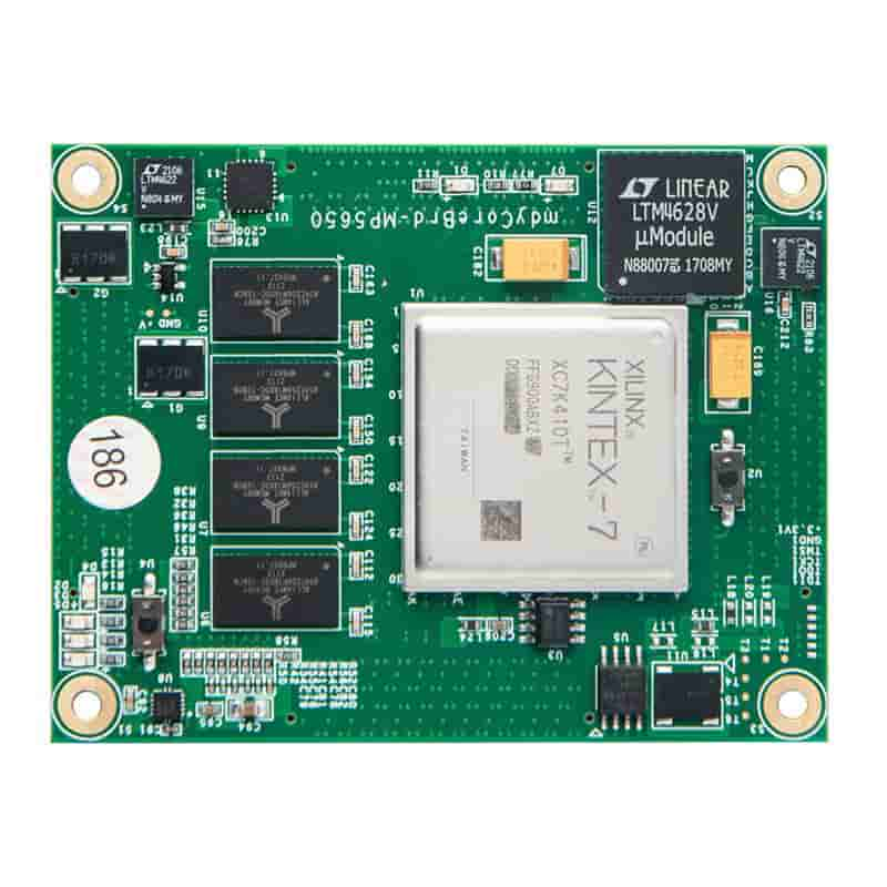
FPGA Xilinx K7 Kintex7 PCIe optical fiber communication
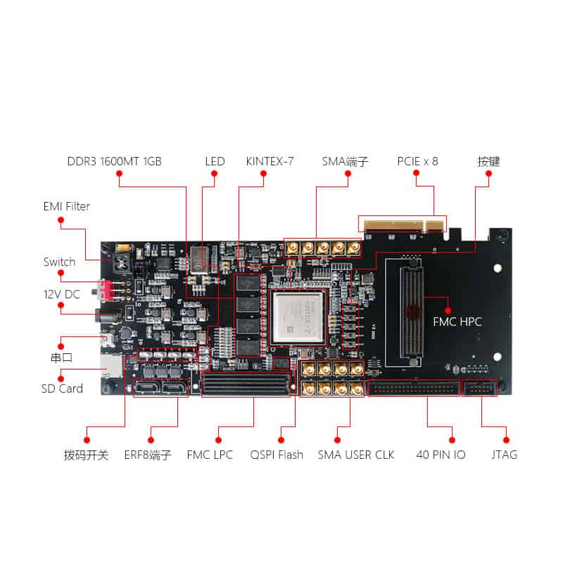
- Micro SD card: Microsd card seat all the way, you can connect the standard Microsd card
- Temperature sensor: a temperature sensor chip LM75, which can monitor the environmental temperature around the development board
- FMC extension port: a FMC HPC and a FMCLPC, which can be compatible with various standard expansion board cards
- ERF8 high -speed connection terminal: 2 ERF8 ports, which supports ultra -high -speed signal transmission 40pin extension: reserved a general extension IO interface with 2.54mm40pin, effective O has 17 pairs, support 3.3V
- The peripheral connection of the level and the 5V level can connect the peripheral peripherals of different general -purpose 1O interfaces
- SMA terminal; 13 high -quality gold -plated SMA heads, which is convenient for users to cooperate with high -speed AD/DA FMC expansion cards for signal collection and processing
- Clock Management: Multi -clock source. These include the 200MHz system differential clock source SIT9102
- Differential crystal oscillating: 50MHz crystal and SI5338P programmable clock management chip: also equipped with
- 66MHz EMCCLK. Can accurately adapt to different use clock frequency
- JTAG port: 10 stitches 2.54mm standard JTAG port, for download and debugging of FPGA programs
- Sub -reset voltage monitoring chip: a piece of ADM706R voltage monitoring chip, and the button with the button provides a global reset signal for the system
- LED: 11 LED lights, indicate the power supply of the board card, config_done signal, FMC
- Power indicator signal, and 4 user LED
- Key and switch: 6 keys and 4 switches are FPGA reset buttons,
- Program B button and 4 user keys are composed. 4 single -knife double throw switch
A: PCB : Quantity, Gerber file and Technic requirements(material,surface finish treatment, copper thickness,board thickness ,...).
PCBA: PCB information, BOM, (Testing documents...).
A: Gerber file: CAM350 RS274X
PCB file: Protel 99SE, P-CAD 2001 PCB
BOM: Excel (PDF, word, txt).
A: Your files are held in complete safety and security.We protect the intellectual property for our customers in the whole process.. All documents from customers are never shared with any third parties.
A: There is no MOQ. We are able to handle Small as well as large volume production with flexibility.
A: The shipping cost is determined by the destination, weight, packing size of the goods. Please let us know if you need us to quote you the shipping cost.
A: Yes, we can provide component source, and we also accept component from client.


-

Phone
-

E-mail
-

Whatsapp
-

Skype
-

Skype
-

Skype