


Oem Pcba Customized Assembly Board Pcba Assembly Services
Application:Aerospace, BMS, Communication, Computer, Consumer Electronics, Home appliance, LED, Medical Instruments, Motherboard, Smart electronics, Wireless charging
Feature:Fexible PCB, High density PCB
Insulation Materials:Epoxy Resin, Metal Composite Materials, Organic Resin
Material:Aluminum Covered Copper Foil Layer, Complex, Fiberglass Epoxy, Fiberglass Epoxy Resin & Polyimide Resin, Paper Phenolic Copper Foil Substrate, Synthetic Fiber
Processing Technology:Delay Pressure Foil, Electrolytic Foil
Key Specifications/ Special Features:
We highly appreciated to coming to ours company. Hope we have an opportunity to establish a long term mutual benefit business relationship and friendship with honored you since today.
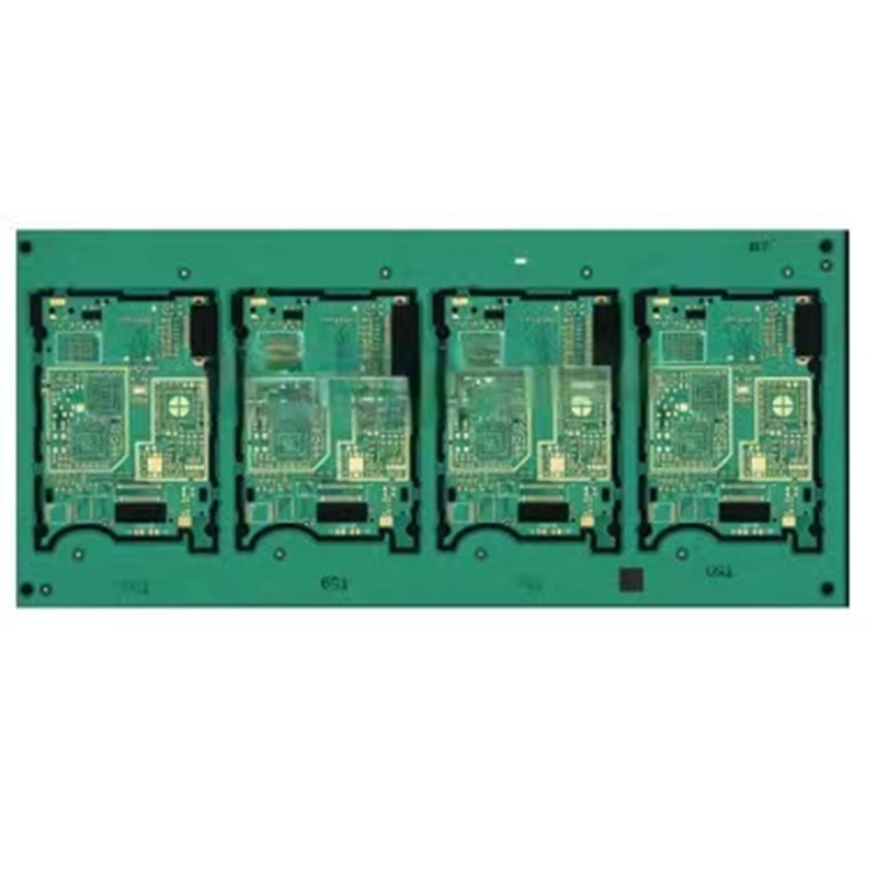
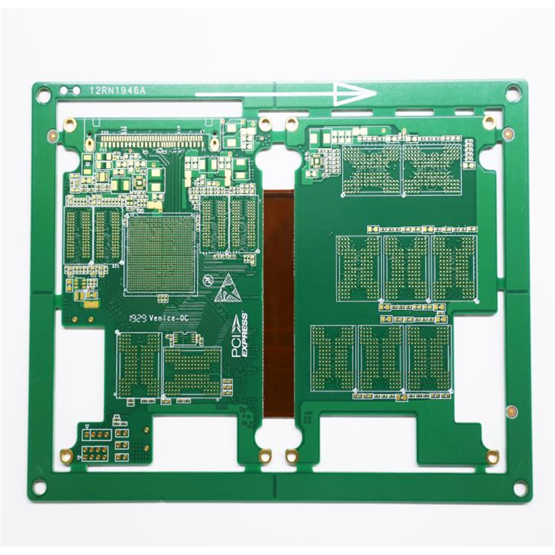
We focus on pcb area around 10 years till now, also we keep ours 2 pcb factory 10 years, 1 focus on 1-30 layers FR4 pcb, 1 focus on 1-4 layers aluminum based pcb & copper based pcb. ours UL # is E479503 . As ours Mature experience and supply chain, we can providing customers the lower cost than the market. Meanwhile we providing 2 years quality warranty to all ours customers and make a 100% inspection before shipment.
As customers PCBA business increasing more, we built ours SMT factory around 5 years in 2018. to providing customers the turnkey PCBA assembly service.
Our capability:
Layer: 1 to 30 layers
Material type: fr-1, fr-2, fr-4, cem-1, cem-3, high TG, fr4 halogen free,
Board thickness: 0.35mm to 3.0mm
Copper thickness: 0.5 oz to 6.0 OZ
Copper thickness in hole: >25.0 um (>1mil)
The max board size:
Board thickness≥1.2mm and not jack panel : 605*530mm.(HASL board: 605*450mm)
Board thickness≥1.2mm jack panel: 550*400mm
Board thickness: 0.5---1.2mm: 400*350mm
Board thickness0.4mm: 350*300mm
Single-sided board: 500*1500mm(board thickness>1.2mm)
Six layer PCB: 430*430mm
Eight layers: 430*430mm
More than eight layers: 270*280mm
Min. drilled hole size: 10mil (0.25mm)
Min. line width: 4mil (0.1mm)
Min. line spacing: 4mil (0.1mm)
Surface finishing: HASL/HASL lead free, HAL, chemical tin, chemical gold, immersion silver/gold, OSP, gold plating
Solder mask color: green/yellow/black/white/red/blue
Tolerance
Shape tolerance: ±0.15
Hole tolerance: PTH: ±0.075 NPTH: ±0.1
PCB packing
Inner packing: vacuum packing / plastic bag
Outer packing: standard carton packing
Certificates: UL, ISO 9001, ISO 14001 , SGS
Profiling: punching, routing, v-cut
Products categories
-

BLS 50A 4-in-1 Governor 2-6S 30.530.5mm racing ...
-

SX1280PA+LNA High power LoRa medical equipment ...
-
5G communication PCB Printed circuit boards us...
-

Gopro3 Dog 3 Brush-less PTZ Two-axis brush-less...
-

65AF405 V2 fly tower 2-6S FPV racing traverser ...
-

32bit 60AF722 V2 Mini fly tower 2-6S FPV Racing...
-

Phone
-

E-mail
-

Whatsapp
-

Skype
-

Skype
-

Skype