One-stop Electronic Manufacturing Services, help you easily achieve your electronic products from PCB & PCBA


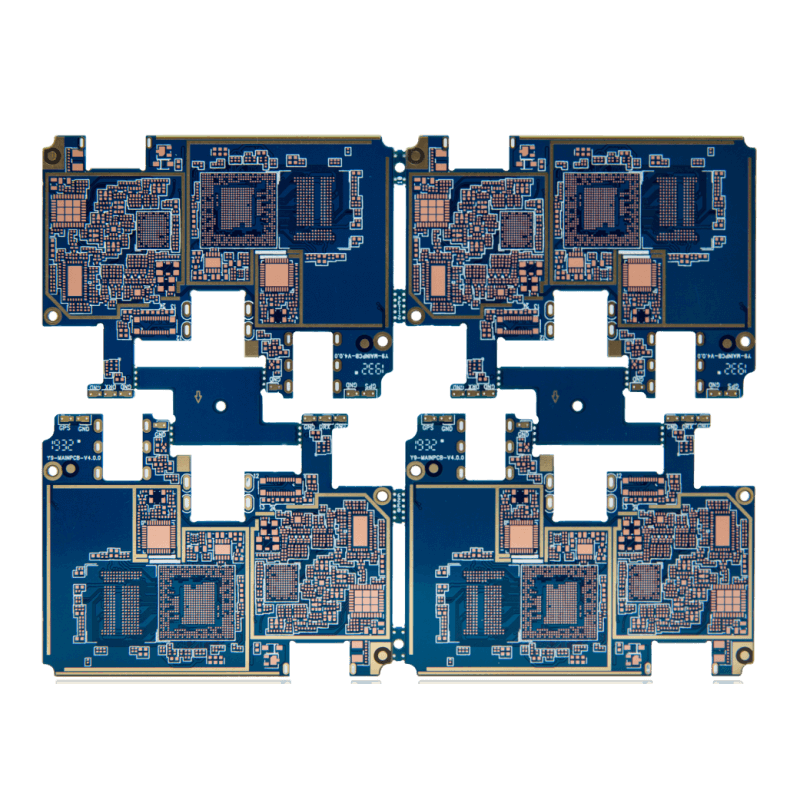
5G communication PCB Printed circuit boards used in 5G communications
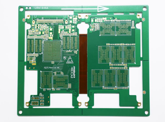
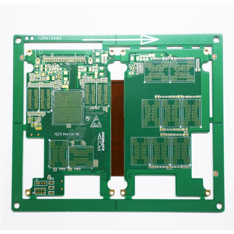
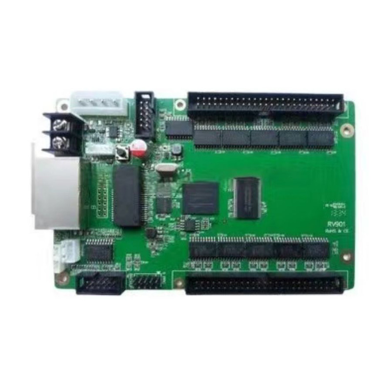
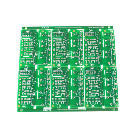
- Applications: Solid state drives
- Number of layers: 12 layers (flexible 2 layers)
- Minimum aperture: 0.2mm
- Plate thickness: 1.6±0.16mm
- Line width line distance: 3.5/4.5mil
- Surface treatment: sunk nickel gold
- Application field: 5G antenna (high frequency mixed voltage)
- Number of floors: 4
- Plate thickness: 1.2mm
- Line width Line distance: /
- Surface treatment: Tin
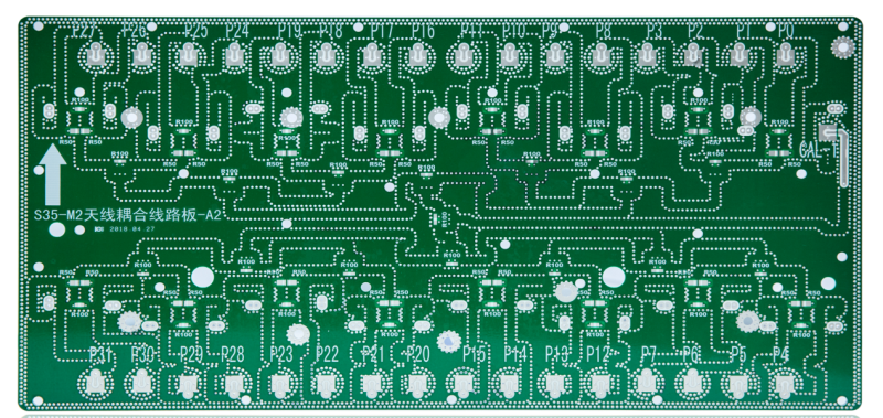
- Application field: 5G antenna
- Number of floors: 4
- Plate thickness: 1.8±0.1mm
- Line width line distance: 70.59/10mil
- Surface treatment: Tin
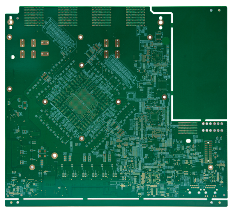
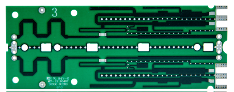
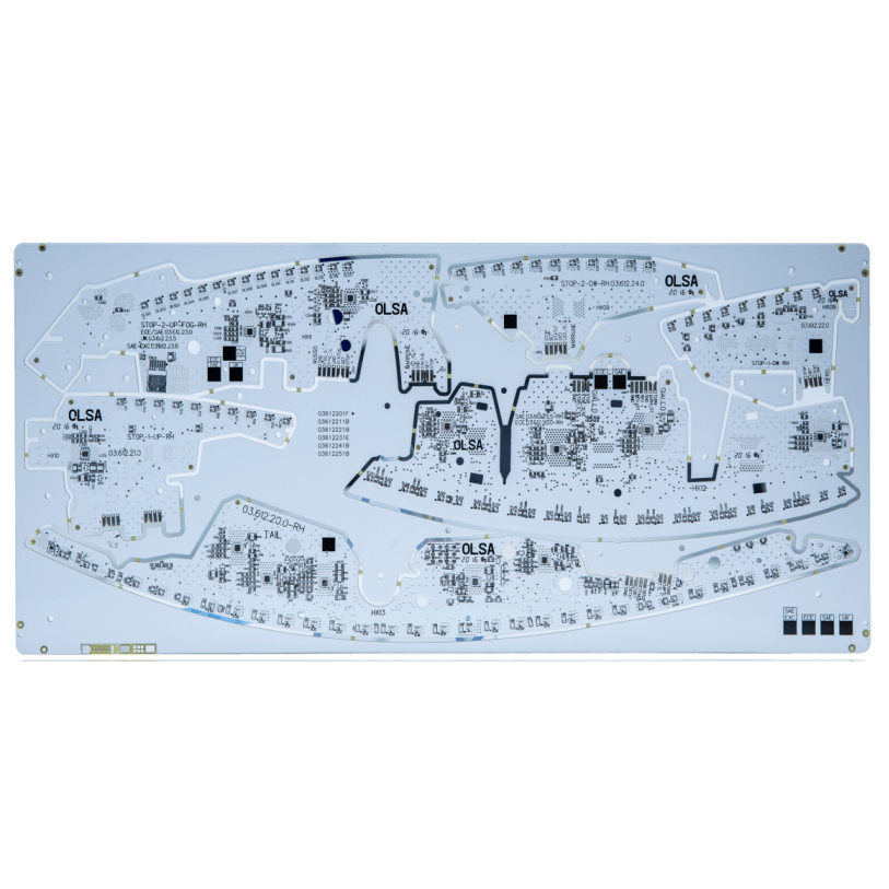
- Application field: communication server
- Number of floors: 24
- Plate thickness: 5.6mm
- Line width line distance: 4/4mil
- Surface treatment: Sunk gold
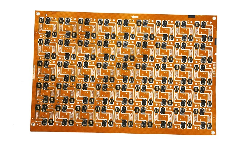
- Application: Fingerprint softboard under the mobile screen
- Type number: GRS02N09788B0
- Number of floors: 2
- Plate thickness: 0.10mm
- Plate: Taihong 2FPDE0803MW
- Line width line distance: 0.05mm
- Minimum aperture: 0.15mm
- Surface treatment: sunk nickel palladium
Write your message here and send it to us
Products categories


-

Phone
-

E-mail
-

Whatsapp
-

Skype
-

Skype
-

Skype