

Compared with silicon-based power semiconductors, SiC (silicon carbide) power semiconductors have significant advantages in switching frequency, loss, heat dissipation, miniaturization, etc.
With the large-scale production of silicon carbide inverters by Tesla, more companies have also begun to land silicon carbide products.
SiC is so “amazing”, how on earth was it made? What are the applications now? Let’s see!
01 ☆ Birth of a SiC
Like other power semiconductors, the SiC-MOSFET industry chain includes the long crystal – substrate – epitaxy – design – manufacturing – packaging link.
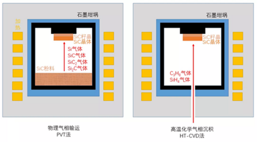
Long crystal
During the long crystal link, unlike the preparation of the Tira method used by single crystal silicon, silicon carbide mainly adopts physical gas transportation method (PVT, also known as improved Lly or seed crystal sublimation method), high temperature chemical gas deposition method ( HTCVD) supplements.
☆ Core step
1. Carbonic solid raw material;
2. After heating, the carbide solid becomes gas;
3. Gas move to the surface of the seed crystal;
4. Gas grows on the surface of the seed crystal into a crystal.
Picture source: “Technical Point to disassemble PVT growth silicon carbide”
Different craftsmanship has caused two major disadvantages compared to the silicon base:
First, production is difficult and the yield is low. The temperature of the carbon -based gas phase grows above 2300 ° C and the pressure is 350MPa. The whole dark box is carried out, and it is easy to mix into impurities. The yield is lower than the silicon base. The larger the diameter, the lower the yield.
The second is slow growth. The Governance of the PVT method is very slow, the speed is about 0.3-0.5mm/h, and it can grow 2cm in 7 days. The maximum can only grow 3-5cm, and the diameter of the crystal ingot is mostly 4 inches and 6 inches.
The Silicon-based 72H can grow to a height of 2-3m, with diameters mostly 6 inches and 8-inch new production capacity for 12 inches. Therefore, silicon carbide is often called crystal ingot, and silicon becomes a crystal stick.
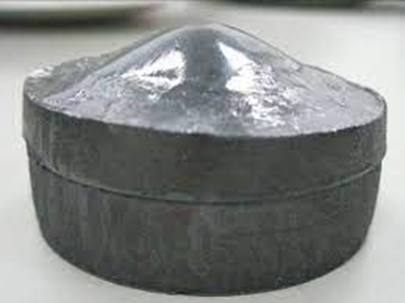
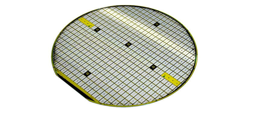
Carbide silicon crystal ingots
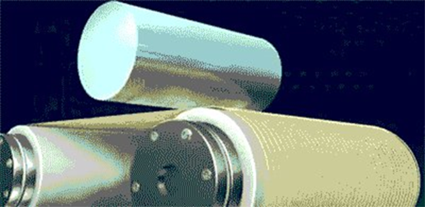
Substrate
After the long crystal is completed, it enters the production process of the substrate.
After targeted cutting, grinding (rough grinding, fine grinding), polishing (mechanical polishing), ultra -precision polishing (chemical mechanical polishing), the silicon carbide substrate is obtained.
The substrate mainly plays the role of physical support, thermal conductivity and conductivity. The difficulty of processing is that the silicon carbide material is high, crispy, and stable in chemical properties. Therefore, traditional silicon -based processing methods are not suitable for silicon carbide substrate.
The quality of the cutting effect directly affects the performance and utilization efficiency (cost) of silicon carbide products, so it is required to be small, uniform thickness, and low cutting.
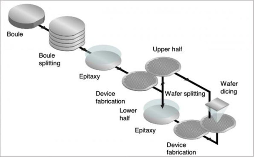
At present, 4 -inch and 6 -inch mainly uses multi -line cutting equipment, cutting silicon crystals into thin slices with a thickness of no more than 1mm.
Multi -line cutting schematic diagram
In the future, with the increase in the size of carbonized silicon wafers, the increase in material utilization requirements will increase, and technologies such as laser slicing and cold separation will also gradually be applied.
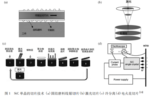
In 2018, Infineon acquired Siltectra GmbH, which developed an innovative process known as cold cracking.
Compared with the traditional multi-wire cutting process loss of 1/4, the cold cracking process only lost 1/8 of the silicon carbide material.
Extension
Since the silicon carbide material cannot make power devices directly on the substrate, various devices are required on the extension layer.
Therefore, after the production of the substrate is completed, a specific single crystal thin film is grown on the substrate through the extension process.
At present, the chemical gas deposition method (CVD) process is mainly used.
Design
After the substrate is made, it enters the product design stage.
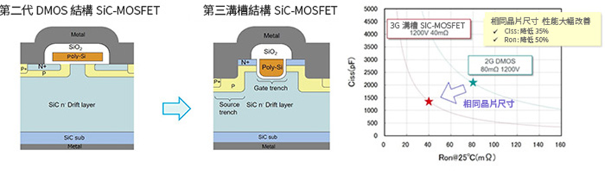
For MOSFET, the focus of the design process is the design of the groove, on the one hand to avoid patent infringement (Infineon, Rohm, ST, etc., have patent layout), and on the other hand to meet the manufacturability and manufacturing costs.
Wafer fabrication
After the product design is completed, it enters the wafer manufacturing stage, and the process is roughly similar to that of silicon, which mainly has the following 5 steps.
☆Step 1: Inject the mask
A layer of silicon oxide (SiO2) film is made, the photoresist is coated, the photoresist pattern is formed through the steps of homogenization, exposure, development, etc., and the figure is transferred to the oxide film through the etching process.

☆Step 2: Ion implantation
The masked silicon carbide wafer is placed into an ion implanter, where aluminum ions are injected to form a P-type doping zone, and annealed to activate the implanted aluminum ions.
The oxide film is removed, nitrogen ions are injected into a specific region of the P-type doping region to form an N-type conductive region of the drain and source, and the implanted nitrogen ions are annealed to activate them.

☆Step 3: Make the grid
Make the grid. In the area between the source and drain, the gate oxide layer is prepared by high temperature oxidation process, and the gate electrode layer is deposited to form the gate control structure.

☆Step 4: Making passivation layers
Passivation layer is made. Deposit a passivation layer with good insulation characteristics to prevent interelectrode breakdown.
☆Step 5: Make drain-source electrodes
Make drain and source. The passivation layer is perforated and metal is sputtered to form a drain and a source.
Photo Source: Xinxi Capital
Although there is little difference between the process level and silicon based, due to the characteristics of silicon carbide materials, ion implantation and annealing need to be carried out in a high temperature environment (up to 1600 ° C), high temperature will affect the lattice structure of the material itself, and the difficulty will also affect the yield.
In addition, for MOSFET components, the quality of gate oxygen directly affects the channel mobility and gate reliability, because there are two kinds of silicon and carbon atoms in the silicon carbide material.
Therefore, a special gate medium growth method is required (another point is that the silicon carbide sheet is transparent, and the position alignment at the photolithography stage is difficult to silicon).
After the wafer manufacturing is completed, the individual chip is cut into a bare chip and can be packaged according to the purpose. The common process for discrete devices is TO package.
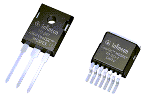
650V CoolSiC™ MOSFETs in TO-247 package
Photo: Infineon
The automotive field has high power and heat dissipation requirements, and sometimes it is necessary to directly build bridge circuits (half bridge or full bridge, or directly packaged with diodes).
Therefore, it is often packaged directly into modules or systems. According to the number of chips packaged in a single module, the common form is 1 in 1 (BorgWarner), 6 in 1 (Infineon), etc., and some companies use a single-tube parallel scheme.
Borgwarner Viper
Supports double-sided water cooling and SiC-MOSFET
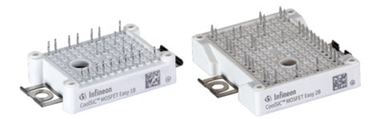
Infineon CoolSiC™ MOSFET modules
Unlike silicon, silicon carbide modules operate at a higher temperature, about 200 ° C.
Traditional soft solder temperature melting point temperature is low, can not meet the temperature requirements. Therefore, silicon carbide modules often use low-temperature silver sintering welding process.
After the module is completed, it can be applied to the parts system.
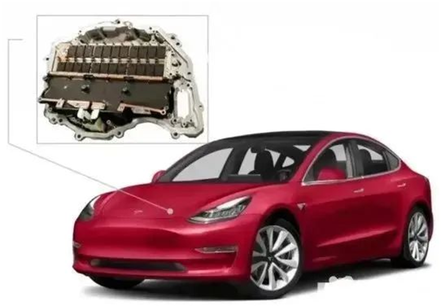
Tesla Model3 motor controller
The bare chip comes from ST, self-developed package and electric drive system
☆02 Application status of SiC?
In the automotive field, power devices are mainly used in DCDC, OBC, motor inverters, electric air conditioning inverters, wireless charging and other parts that require AC/DC fast conversion (DCDC mainly acts as a fast switch).
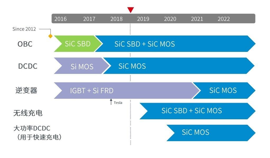
Photo: BorgWarner
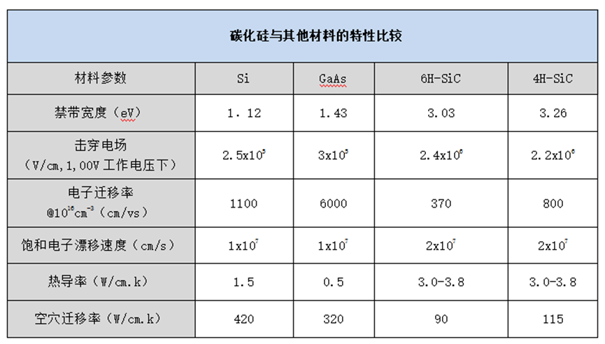
Compared with silicon-based materials, SIC materials have higher critical avalanche breakdown field strength (3×10⁶V/cm), better thermal conductivity (49W/mK) and wider band gap (3.26eV).
The wider the band gap, the smaller the leakage current and the higher the efficiency. The better the thermal conductivity, the higher the current density. The stronger the critical avalanche breakdown field is, the voltage resistance of the device can be improved.
Therefore, in the field of on-board high voltage, MOSFETs and SBD prepared by silicon carbide materials to replace the existing silicon-based IGBT and FRD combination can effectively improve power and efficiency, especially in high frequency application scenarios to reduce switching losses.
At present, it is most likely to achieve large-scale applications in motor inverters, followed by OBC and DCDC.
800V voltage platform
In the 800V voltage platform, the advantage of high frequency makes enterprises more inclined to choose SiC-MOSFET solution. Therefore, most of the current 800V electronic control planning SiC-MOSFET.
Platform-level planning includes modern E-GMP, GM Otenergy – pickup field, Porsche PPE, and Tesla EPA. Except for Porsche PPE platform models that do not explicitly carry SiC-MOSFET (the first model is silica-based IGBT), other vehicle platforms adopt SiC-MOSFET schemes.

Universal Ultra energy platform
800V model planning is more, the Great Wall Salon brand Jiagirong, Beiqi pole Fox S HI version, ideal car S01 and W01, Xiaopeng G9, BMW NK1, Changan Avita E11 said that it will carry 800V platform, in addition to BYD, Lantu, GAC ‘an, Mercedes-Benz, zero Run, FAW Red Flag, Volkswagen also said 800V technology in research.
From the situation of 800V orders obtained by Tier1 suppliers, BorgWarner, Wipai Technology, ZF, United Electronics, and Huichuan all announced 800V electric drive orders.
400V voltage platform
In the 400V voltage platform, SiC-MOSFET is mainly in the consideration of high power and power density and high efficiency.
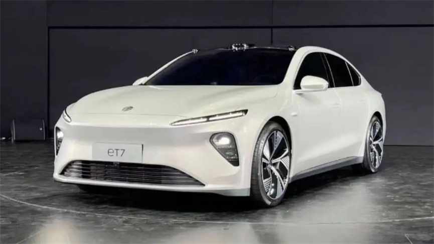
Such as the Tesla Model 3\Y motor that has been mass-produced now, the peak power of BYD Hanhou motor is about 200Kw (Tesla 202Kw, 194Kw, 220Kw, BYD 180Kw), NIO will also use SiC-MOSFET products starting from ET7 and the ET5 that will be listed later. Peak power is 240Kw (ET5 210Kw).
In addition, from the perspective of high efficiency, some enterprises are also exploring the feasibility of auxiliary flooding SiC-MOSFET products.
Post time: Jul-08-2023


