

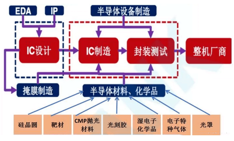
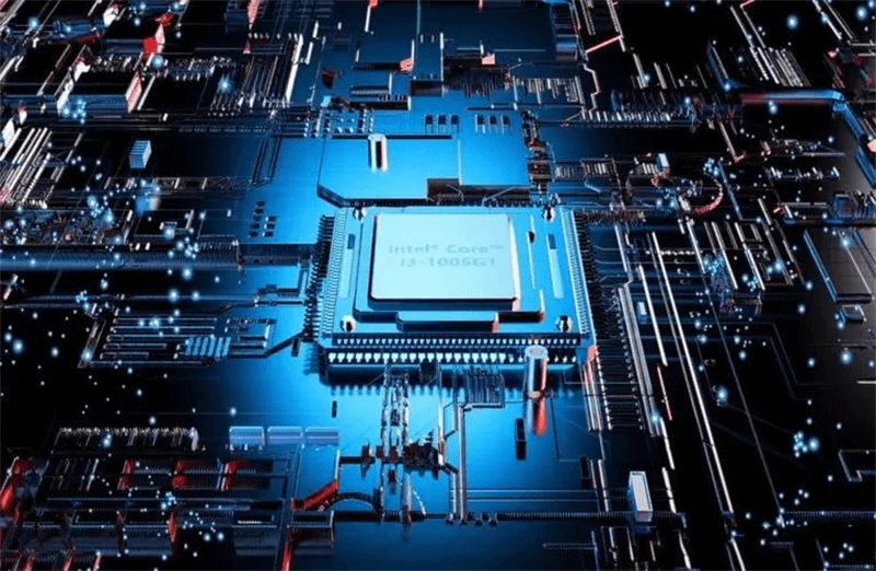
From a professional perspective, the production process of a chip is extremely complicated and tedious. However, from the complete industrial chain of IC, it is mainly divided into four parts: IC design → IC manufacturing → packaging → testing.
Chip production process:
1. Chip design
The chip is a product with small volume but extremely high precision. To make a chip, design is the first part. The design requires the help of the chip design of the chip design required for processing with the help of the EDA tool and some IP cores.

Chip production process:
1. Chip design
The chip is a product with small volume but extremely high precision. To make a chip, design is the first part. The design requires the help of the chip design of the chip design required for processing with the help of the EDA tool and some IP cores.

3. Silicon -lifting
After the silicon is separated, the remaining materials are abandoned. Pure silicon after multiple steps has reached the quality of semiconductor manufacturing. This is the so -called electronic silicon.
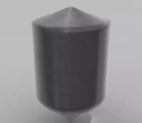
4. Silicon -casting ingots
After purifying, the silicon should be cast into silicon ingots. A single crystal of an electronic -grade silicon after being cast into ingot weighs about 100 kg, and the purity of silicon reaches 99.9999%.
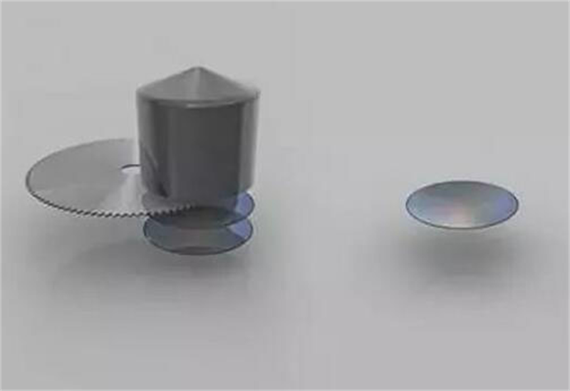
5. File processing
After the silicon ingot is cast, the entire silicon ingot must be cut into pieces, which is the wafer that we commonly call the wafer, which is very thin. Subsequently, the wafer is polished until perfect, and the surface is as smooth as the mirror.
The diameter of silicon wafers is 8 -inch (200mm) and 12 -inch (300mm) in diameter. The larger the diameter, the lower the cost of a single chip, but the higher the processing difficulty.
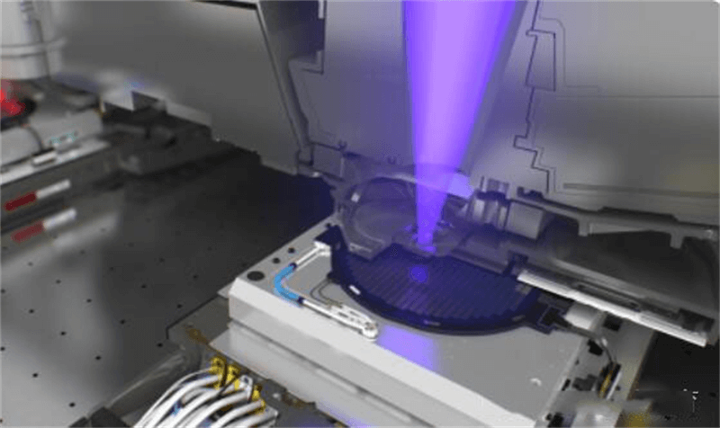
7. Eclipse and ion injection
First, it is necessary to corrode silicon oxide and silicon nitride exposed outside the photoresist, and precipitate a layer of silicon to insulate between the crystal tube, and then use the etching technology to expose the bottom silicon. Then inject the boron or phosphorus into the silicon structure, then fill the copper to connect with other transistors, and then apply another layer of glue on it to make a layer of structure. Generally, a chip contains dozens of layers, like densely intertwined highways.
Post time: Jul-08-2023


