

Why learn power circuit design
The power supply circuit is an important part of an electronic product, the design of the power supply circuit is directly related to the performance of the product.
Classification of power supply circuits
The power circuits of our electronic products mainly include linear power supplies and high-frequency switching power supplies. In theory, the linear power supply is how much current the user needs, the input will provide how much current; Switching power supply is how much power the user needs, and how much power is provided at the input end.
Schematic diagram of linear power supply circuit
Linear power devices work in a linear state, such as our commonly used voltage regulator chips LM7805, LM317, SPX1117 and so on. Figure 1 below is the schematic diagram of the LM7805 regulated power supply circuit.
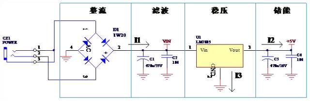
Figure 1 Schematic diagram of linear power supply
It can be seen from the figure that the linear power supply is composed of functional components such as rectification, filtering, voltage regulation and energy storage. At the same time, the general linear power supply is a series voltage regulation power supply, the output current is equal to the input current, I1=I2+I3, I3 is the reference end, the current is very small, so I1≈I3. Why do we want to talk about the current, because PCB design, the width of each line is not randomly set, is to be determined according to the size of the current between the nodes in the schematic. The current size and current flow should be clear to make the board just right.
Linear power supply PCB diagram
When designing the PCB, the layout of the components should be compact, all the connections should be as short as possible, and the components and lines should be laid out according to the functional relationship of the schematic components. This power supply diagram is the first rectification, and then filtering, filtering is the voltage regulation, voltage regulation is the energy storage capacitor, after flowing through the capacitor to the following circuit electricity.
Figure 2 is the PCB diagram of the above schematic diagram, and the two diagrams are similar. The left picture and the right picture are a little different, the power supply in the left picture is directly to the input foot of the voltage regulator chip after rectification, and then the voltage regulator capacitor, where the filtering effect of the capacitor is much worse, and the output is also problematic. The picture on the right is a good one. We must not only consider the flow of the positive power supply problem, but also must consider the backflow problem, in general, the positive power line and the ground backflow line should be as close to each other as possible.
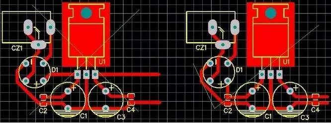
Figure 2 PCB diagram of linear power supply
When designing the linear power supply PCB, we should also pay attention to the heat dissipation problem of the power regulator chip of the linear power supply, how the heat comes, if the voltage regulator chip front end is 10V, the output end is 5V, and the output current is 500mA, then there is a 5V voltage drop on the regulator chip, and the heat generated is 2.5W; If the input voltage is 15V, the voltage drop is 10V, and the heat generated is 5W, therefore, we need to set aside enough heat dissipation space or reasonable heat sink according to the heat dissipation power. Linear power supply is generally used in situations where the pressure difference is relatively small and the current is relatively small, otherwise, please use the switching power supply circuit.
High frequency switching power supply circuit schematic example
Switching power supply is to use the circuit to control the switching tube for high-speed on-off and cut-off, generate PWM waveform, through the inductor and the continuous current diode, the use of electromagnetic conversion of the way to regulate voltage. Switching power supply, high efficiency, low heat, we generally use the circuit: LM2575, MC34063, SP6659 and so on. In theory, the switching power supply is equal at both ends of the circuit, the voltage is inversely proportional, and the current is inversely proportional.
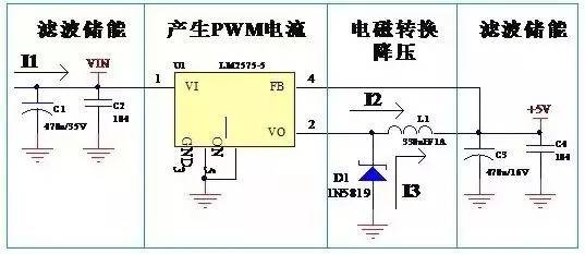
Figure 3 Schematic diagram of LM2575 switching power supply circuit
PCB diagram of switching power supply
When designing the PCB of the switching power supply, it is necessary to pay attention to: the input point of the feedback line and the continuous current diode are for whom the continuous current is given. As can be seen from Figure 3, when U1 is switched on, the current I2 enters the inductor L1. The characteristic of the inductor is that when the current flows through the inductor, it cannot be generated suddenly, nor can it disappear suddenly. The change of current in the inductor has a time process. Under the action of pulsed current I2 flowing through the inductance, some of the electrical energy is converted into magnetic energy, and the current gradually increases, at a certain time, the control circuit U1 turns off I2, due to the characteristics of inductance, the current can not suddenly disappear, at this time the diode works, it takes over the current I2, so it is called the continuous current diode, it can be seen that the continuous current diode is used for the inductance. The continuous current I3 starts from the negative end of C3 and flows into the positive end of C3 through D1 and L1, which is equivalent to a pump, using the energy of the inductor to increase the voltage of the capacitor C3. There is also the problem of the input point of the feedback line of voltage detection, which should be fed back to the place after filtering, otherwise the output voltage ripple will be larger. These two points are often ignored by many of our PCB designers, thinking that the same network is not the same there, in fact, the place is not the same, and the performance impact is great. Figure 4 is the PCB diagram of LM2575 switching power supply. Let’s see what is wrong with the wrong diagram.
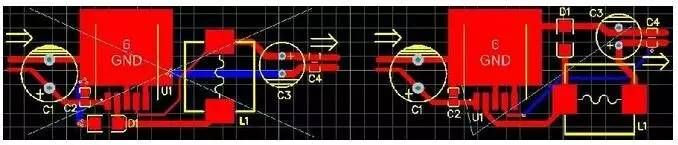
Figure 4 PCB diagram of LM2575 switching power supply
Why do we want to talk about the schematic principle in detail, because the schematic contains a lot of PCB information, such as the access point of the component pin, the current size of the node network, etc., see the schematic, PCB design is not a problem. The LM7805 and LM2575 circuits represent the typical layout circuit of linear power supply and switching power supply, respectively. When making PCBS, the layout and wiring of these two PCB diagrams are directly on the line, but the products are different and the circuit board is different, which is adjusted according to the actual situation.
All changes are inseparable, so the principle of the power circuit and the way the board is so, and every electronic product is inseparable from the power supply and its circuit, therefore, learn the two circuits, the other is also understood.
Post time: Jul-04-2023


