

Note the following considerations for the clock on a board:
1. Layout
a, the clock crystal and related circuits should be arranged in the central position of the PCB and have a good formation, rather than near the I/O interface. The clock generation circuit cannot be made into a daughter card or daughter board form, must be made on a separate clock board or carrier board.
As shown in the following figure, the green box part of the next layer is good not to walk the line
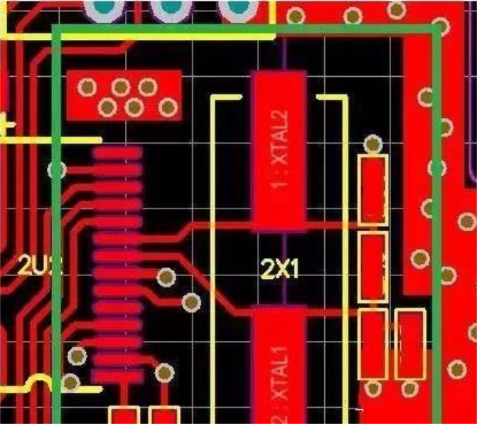
b, only the devices related to the clock circuit in the PCB clock circuit area, avoid laying other circuits, and do not lay other signal lines near or below the crystal: Using the ground plane under a clock-generating circuit or crystal, if other signals pass through the plane, which violates the mapped plane function, if the signal passes through the ground plane, there will be a small ground loop and affect the continuity of the ground plane, and these ground loops will cause problems at high frequencies.
c. For clock crystals and clock circuits, shielding measures can be adopted for shielding processing;
d, if the clock shell is metal, the PCB design must be laid under the crystal copper, and ensure that this part and the complete ground plane has a good electrical connection (through porous ground).
Benefits of paving under clock crystals:
The circuit inside the crystal oscillator generates RF current, and if the crystal is enclosed in a metal housing, the DC power pin is the reliance of the DC voltage reference and the RF current loop reference inside the crystal, releasing the transient current generated by the RF radiation of the housing through the ground plane. In short, the metal shell is a single-ended antenna, and the near image layer, ground plane layer and sometimes two or more layers are sufficient for the radiative coupling of the RF current to the ground. The crystal floor is also good for heat dissipation. The clock circuit and crystal underlay will provide a mapping plane, which can reduce the common mode current generated by the associated crystal and clock circuit, thus reducing RF radiation. The ground plane also absorbs the differential mode RF current. This plane must be connected to the complete ground plane by multiple points and requires multiple through-holes, which can provide low impedance. To enhance the effect of this ground plane, the clock generator circuit should be close to this ground plane.
Smt-packaged crystals will have more RF energy radiation than metal-clad crystals: Because surface mounted crystals are mostly plastic packages, the RF current inside the crystal will radiate into space and coupled to other devices.
1. Share the clock routing
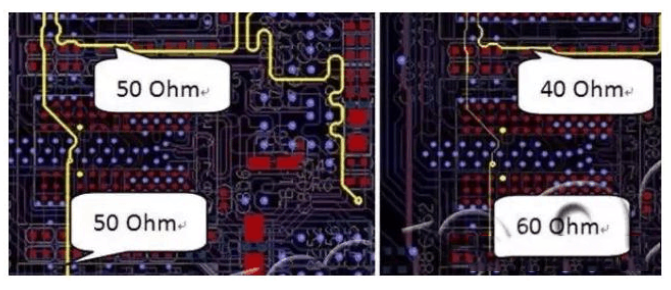
It is better to connect the fast rising edge signal and the bell signal with radial topology than to connect the network with a single common driver source, and each route should be routed by terminating measures according to its characteristic impedance.
2, clock transmission line requirements and PCB layering
Clock routing principle: Arrange a complete image plane layer in the immediate vicinity of the clock routing layer, reduce the length of the line and carry out impedance control.
Incorrect cross-layer wiring and impedance mismatches can result in:
1) The use of holes and jumps in the wiring lead to the imintegrity of the image loop;
2) The surge voltage on the image plane due to the voltage on the device signal pin changes with the change of the signal;
3), if the line does not consider the 3W principle, different clock signals will cause crosstalk;
Wiring of the clock signal
1, the clock line must walk in the inner layer of the multi-layer PCB board. And be sure to follow a ribbon line; If you want to walk on the outer layer, only microstrip line.
2, the inner layer can ensure a complete image plane, it can provide a low-impedance RF transmission path, and generate magnetic flux to offset the magnetic flux of their source transmission line, the closer the distance between the source and the return path, the better the degaussing. Thanks to enhanced demagnetization, each full planar image layer of a high-density PCB provides 6-8dB suppression.
3, the advantages of multi-layer board: there is a layer or multiple layers can be dedicated to the complete power supply and ground plane, can be designed into a good decoupling system, reduce the area of the ground loop, reduce the differential mode radiation, reduce EMI, reduce the impedance level of the signal and power return path, can maintain the consistency of the entire line impedance, reduce the crosstalk between the adjacent lines.
Post time: Jul-05-2023


