

1. General practice
In the PCB design, in order to make the high frequency circuit board design more reasonable, better anti-interference performance, should be considered from the following aspects:
(1) Reasonable selection of layers When routing high-frequency circuit boards in PCB design, the inner plane in the middle is used as the power and ground layer, which can play a shielding role, effectively reduce the parasitic inductance, shorten the length of signal lines, and reduce the cross interference between signals.
(2) Routing mode Routing mode must be in accordance with 45° Angle turning or arc turning, which can reduce high-frequency signal emission and mutual coupling.
(3) Cable length The shorter the cable length, the better. The shorter the parallel distance between two wires, the better.
(4) Number of through holes The fewer the number of through holes, the better.
(5) Interlayer wiring direction The direction of interlayer wiring should be vertical, that is, the top layer is horizontal, the bottom layer is vertical, so as to reduce the interference between signals.
(6) Copper coating increased grounding copper coating can reduce the interference between signals.
(7) The inclusion of the important signal line processing, can significantly improve the anti-interference ability of the signal, of course, can also be the inclusion of the interference source processing, so that it can not interfere with other signals.
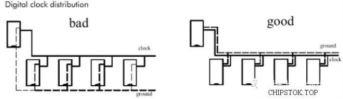
(8)Signal cables do not route signals in loops. Route signals in Daisy chain mode.
2. Wiring priority
Key signal line priority: analog small signal, high-speed signal, clock signal and synchronization signal and other key signals priority wiring
Density first principle: Start wiring from the most complex connections on the board. Start wiring from the most densely wired area of the board
Points to note:
A. Try to provide a special wiring layer for key signals such as clock signals, high-frequency signals and sensitive signals, and ensure the minimum loop area. If necessary, manual priority wiring, shielding and increasing safety spacing should be adopted. Ensure signal quality.
b. EMC environment between the power layer and the ground is poor, so signals sensitive to interference should be avoided.
c. The network with impedance control requirements should be wired as far as possible according to the line length and line width requirements.
3, clock wiring
The clock line is one of the biggest factors affecting EMC. Make fewer holes in the clock line, avoid walking with other signal lines as far as possible, and stay away from general signal lines to avoid interference with signal lines. At the same time, the power supply on the board should be avoided to prevent interference between the power supply and the clock.
If there is a special clock chip on the board, it can not go under the line, should be laid under the copper, if necessary, can also be special to its land. For many chip reference crystal oscillator, these crystal oscillator should not be under the line, to lay copper isolation.
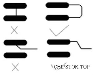
4. Line at right angles
Right-angle cabling is generally required to avoid the situation in PCB wiring, and has almost become one of the standards to measure the quality of wiring, so how much impact will right-angle cabling have on signal transmission? In principle, right-angle routing will cause the line width of the transmission line to change, resulting in impedance discontinuity. In fact, not only right Angle routing, ton Angle, acute Angle routing may cause impedance changes.
The influence of right-angle routing on signal is mainly reflected in three aspects:
First, the corner can be equivalent to the capacitive load on the transmission line, slowing down the rise time;
Second, impedance discontinuity will cause signal reflection;
Third, EMI produced by the right Angle tip.
5. Acute Angle
(1) For high frequency current, when the turning point of the wire presents a right Angle or even an acute Angle, near the corner, the magnetic flux density and electric field intensity are relatively high, will radiation strong electromagnetic wave, and the inductance here will be relatively large, the inductive will be larger than the obtuse Angle or rounded Angle.
(2) For the bus wiring of the digital circuit, the wiring corner is obtuse or rounded, the area of the wiring is relatively small. Under the same line spacing condition, the total line spacing takes up 0.3 times less width than the right Angle turn.
6. Differential routing
Cf. Differential wiring and impedance matching
Differential Signal is used more and more widely in the design of high-speed circuits, because the most important signals in circuits always use differential structure. Definition: In plain English, it means that the driver sends two equivalent, inverting signals, and the receiver determines whether the logical state is “0″ or “1″ by comparing the difference between the two voltages. The pair carrying the differential signal is called differential routing.
Compared with ordinary single-ended signal routing, differential signal has the most obvious advantages in the following three aspects:
a. Strong anti-interference ability, because the coupling between the two differential wires is very good, when there is noise interference from the outside, it is almost coupled to the two lines at the same time, and the receiver only cares about the difference between the two signals, so the common mode noise from the outside can be completely cancelled out.
b. can effectively inhibit EMI. Similarly, because the polarity of two signals is opposite, the electromagnetic fields radiated by them can cancel each other. The closer the coupling, the less electromagnetic energy released to the outside world.
c. Precise timing positioning. Since the switching changes of differential signals are located at the intersection of two signals, unlike ordinary single-ended signals which rely on high and low threshold voltage, the impact of technology and temperature is small, which can reduce the errors in timing and is more suitable for circuits with low amplitude signals. LVDS (low voltage differential signaling), which is popular at present, refers to this small amplitude differential signaling technology.
For PCB engineers, the most important thing is to ensure that the advantages of differential routing can be fully utilized in the actual routing. Perhaps as long as the contact with Layout people will understand the general requirements of differential routing, that is, “equal length, equal distance”.
The equal length is to ensure that the two differential signals maintain opposite polarity at all times and reduce the common-mode component. Equidistance is mainly to ensure that the difference impedance is consistent and reduce reflection. “As close as possible” is sometimes a requirement for differential routing.
7. Snake line
Serpentine line is a kind of Layout which is often used in layout. Its main purpose is to adjust the delay and meet the requirements of system timing design. The first thing designers need to realize is that snake-like wires can destroy signal quality and change transmission delay, and should be avoided when wiring. However, in actual design, in order to ensure sufficient holding time of signals, or to reduce the time offset between the same group of signals, it is often necessary to deliberately wind.
Points to note:
Pairs of differential signal lines, generally parallel lines, as little as possible through the hole, must be punched, should be two lines together, in order to achieve impedance matching.
A group of buses with the same attributes should be routed side by side as far as possible to achieve equal length. The hole leading from the patch pad is as far away from the pad as possible.
Post time: Jul-05-2023


