

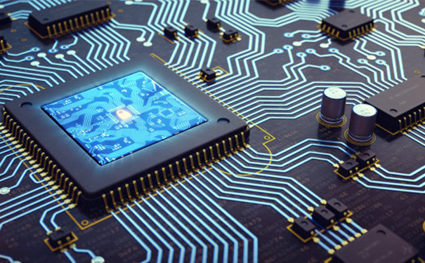
From the development history of chip, the development direction of chip is high speed, high frequency, low power consumption. Chip manufacturing process mainly includes chip design, chip manufacturing, packaging manufacturing, cost testing and other links, among which the chip manufacturing process is particularly complex. Let’s look at the chip manufacturing process, especially the chip manufacturing process.
The first is the chip design, according to the design requirements, the generated “pattern”
1, the raw material of the chip wafer
The composition of wafer is silicon, silicon is refined by quartz sand, the wafer is the silicon element is purified (99.999%), and then the pure silicon is made into silicon rod, which becomes the quartz semiconductor material for the manufacture of integrated circuit, the slice is the specific need of the chip production wafer. The thinner the wafer, the lower the cost of production, but the higher the process requirements.
2.Wafer coating
The wafer coating can resist oxidation and temperature, and the material is a kind of photoresistance.
3, wafer lithography development, etching
The process uses chemicals that are sensitive to UV light, which softens them. The shape of the chip can be obtained by controlling the position of the shading. Silicon wafers are coated with photoresist so that they dissolve in ultraviolet light. This is where the first shading can be applied, so that the part of the UV light is dissolved, which can then be washed away with a solvent. So the rest of it is the same shape as the shade, which is what we want. This gives us the silica layer we need.
4,Add impurities
Ions are implanted into the wafer to generate the corresponding P and N semiconductors.
The process starts with an exposed area on a silicon wafer and is put into a mixture of chemical ions. The process will change the way the dopant zone conducts electricity, allowing each transistor to switch on, off or carry data. Simple chips can use only one layer, but complex chips often have many layers, and the process is repeated over and over again, with the different layers connected by an open window. This is similar to the production principle of the layer PCB board. More complex chips may require multiple layers of silica, which can be achieved through repeated lithography and the process above, forming a three-dimensional structure.
5.Wafer testing
After the above several processes, the wafer formed a lattice of grains. The electrical characteristics of each grain were examined by means of ‘needle measurement’. Generally, the number of grains of each chip is huge, and it is a very complex process to organize a pin test mode, which requires mass production of models with the same chip specifications as far as possible during production. The higher the volume, the lower the relative cost, which is one of the reasons why mainstream chip devices are so cheap.
6. Encapsulation
After the wafer is manufactured, pin is fixed, and various packaging forms are produced according to the requirements. This is the reason why the same chip core can have different packaging forms. For example: DIP, QFP, PLCC, QFN, etc. This is mainly decided by users’ application habits, application environment, market form and other peripheral factors.
7. Testing and packaging
After the above process, the chip manufacturing has been completed, this step is to test the chip, remove the defective products, and packaging.
The above is the related content of chip manufacturing process organized by Create Core Detection. I hope it will help you. Our company has professional engineers and the industry elite team, has 3 standardized laboratories, the laboratory area is more than 1800 square meters, can undertake electronic components testing verification, IC true or false identification, product design material selection, failure analysis, function testing, factory incoming material inspection and tape and other testing projects.
Post time: Jun-12-2023


