

Generally speaking, it is difficult to avoid a small amount of failure in the development, production and use of semiconductor devices. With the continuous improvement of product quality requirements, failure analysis is becoming more and more important. By analyzing specific failure chips, It can help circuit designers find the defects of device design, the mismatch of process parameters, the unreasonable design of peripheral circuit or misoperation caused by the problem. The necessity of failure analysis of semiconductor devices is mainly manifested in the following aspects:
(1) Failure analysis is a necessary means to determine the failure mechanism of the device chip;
(2) Failure analysis provides necessary basis and information for effective fault diagnosis;
(3) Failure analysis provides necessary feedback information for design engineers to continuously improve or repair the chip design and make it more reasonable in accordance with the design specification;
(4) Failure analysis can provide necessary supplement for production test and provide necessary information basis for optimization of verification test process.
For the failure analysis of semiconductor diodes, audions or integrated circuits, electrical parameters should be tested first, and after the appearance inspection under the optical microscope, the packaging should be removed. While maintaining the integrity of the chip function, the internal and external leads, bonding points and the surface of the chip should be kept as far as possible, so as to prepare for the next step of analysis.
Using scanning electron microscopy and energy spectrum to do this analysis: including the observation of the microscopic morphology, failure point search, defect point observation and location, accurate measurement of the device's microscopic geometry size and rough surface potential distribution and the logic judgment of digital gate circuit (with voltage contrast image method); Use energy spectrometer or spectrometer to do this analysis has: microscopic element composition analysis, material structure or pollutant analysis.
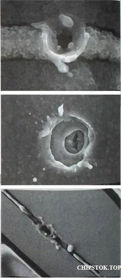
01. Surface defects and burns of semiconductor devices
Surface defects and burn-out of semiconductor devices are both common failure modes, as shown in Figure 1, which is the defect of the purified layer of integrated circuit.
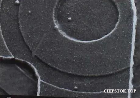
Figure 2 shows the surface defect of the metallized layer of the integrated circuit.
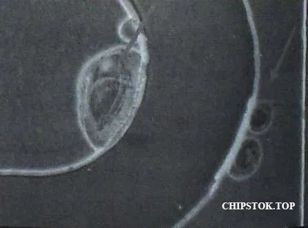
Figure 3 shows the breakdown channel between the two metal strips of the integrated circuit.
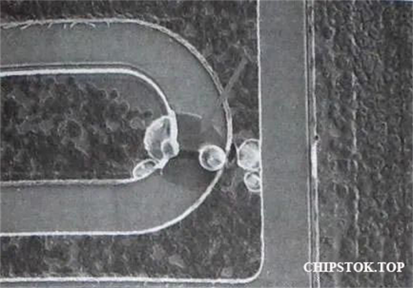
Figure 4 shows the metal strip collapse and skew deformation on the air bridge in the microwave device.
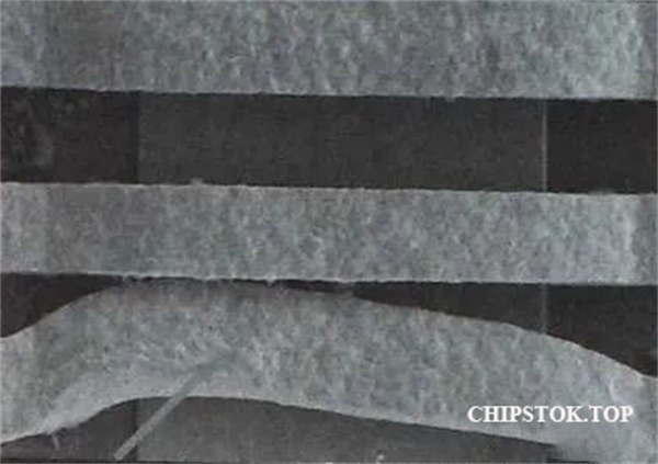
Figure 5 shows the grid burnout of the microwave tube.
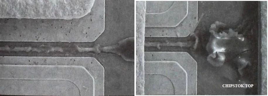
Figure 6 shows the mechanical damage to the integrated electrical metallized wire.
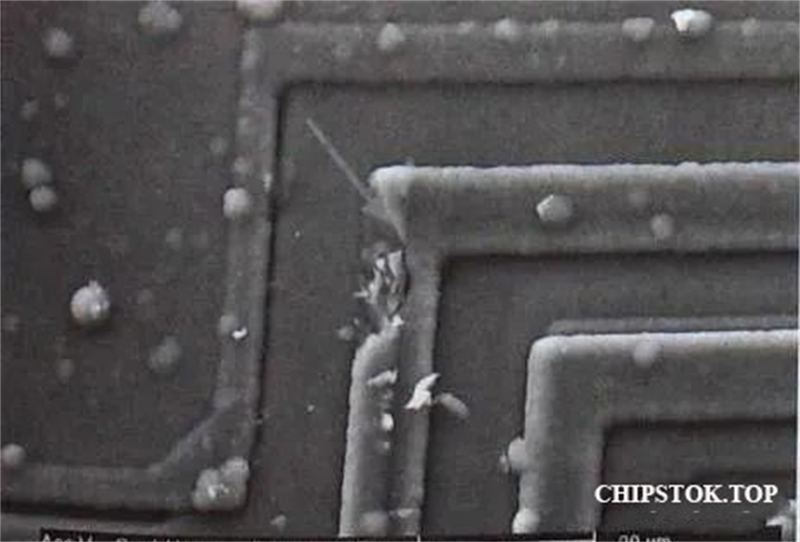
Figure 7 shows the mesa diode chip opening and defect.
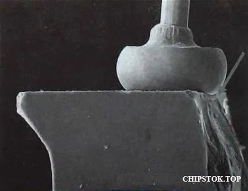
Figure 8 shows the breakdown of the protective diode at the input of the integrated circuit.
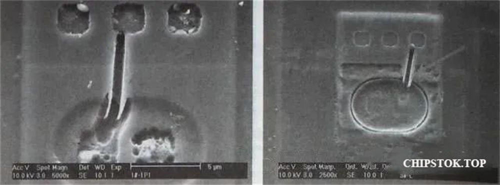
Figure 9 shows that the surface of the integrated circuit chip is damaged by mechanical impact.
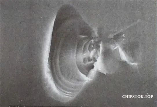
Figure 10 shows the partial burnout of the integrated circuit chip.
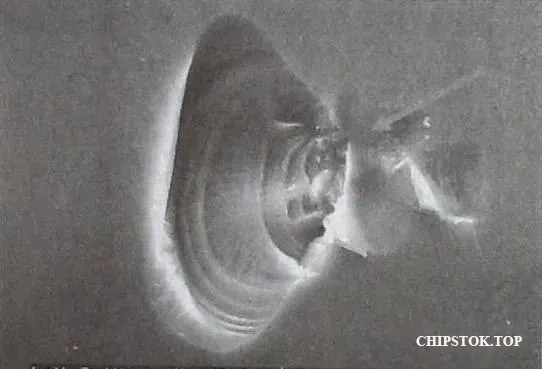
Figure 11 shows the diode chip was broken down and severely burned, and the breakdown points turned into melting state.
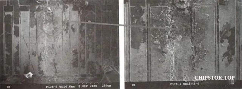
Figure 12 shows the gallium nitride microwave power tube chip burnt, and the burnt point presents a molten sputtering state.
02. Electrostatic breakdown
Semiconductor devices from manufacturing, packaging, transportation until on the circuit board for insertion, welding, machine assembly and other processes are under the threat of static electricity. In this process, transportation is damaged due to frequent movement and easy exposure to the static electricity generated by the outside world. Therefore, special attention should be paid to electrostatic protection during transmission and transportation to reduce losses.
In semiconductor devices with unipolar MOS tube and MOS integrated circuit is particularly sensitive to static electricity, especially MOS tube, because of its own input resistance is very high, and the gate-source electrode capacitance is very small, so it is very easy to be affected by external electromagnetic field or electrostatic induction and charged, and because of the electrostatic generation, it is difficult to discharge charge in time, Therefore, it is easy to cause the accumulation of static electricity to the instantaneous breakdown of the device. The form of electrostatic breakdown is mainly electrical ingenious breakdown, that is, the thin oxide layer of the grid is broken down, forming a pinhole, which shorts the gap between the grid and the source or between the grid and the drain.
And relative to MOS tube MOS integrated circuit antistatic breakdown ability is relatively slightly better, because the input terminal of MOS integrated circuit is equipped with protective diode. Once there is a large electrostatic voltage or surge voltage into most of the protective diodes can be switched to the ground, but if the voltage is too high or the instantaneous amplification current is too large, sometimes the protective diodes will themselves, as shown in Figure 8.
The several pictures shown in figure13 are the electrostatic breakdown topography of MOS integrated circuit. The breakdown point is small and deep, presenting a molten sputtering state.
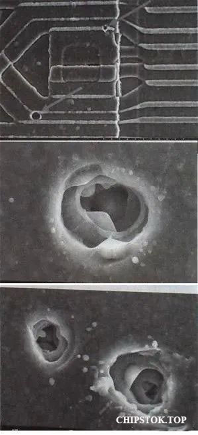
Figure 14 shows the appearance of electrostatic breakdown of the magnetic head of a computer hard disk.
Post time: Jul-08-2023


