

The reasonable layout of electronic components on PCB board is a very important link to reduce welding defects! Components should avoid areas with very large deflection values and high internal stress areas as far as possible, and the layout should be as symmetrical as possible.
In order to maximize the use of circuit board space, I believe that many design partners will try to place the components against the edge of the board, but in fact, this practice will bring great difficulty to the production and PCBA assembly, and even lead to the inability to weld assembly oh!
Today, let's talk about the layout of the edge device in detail
Panel side device layout hazard
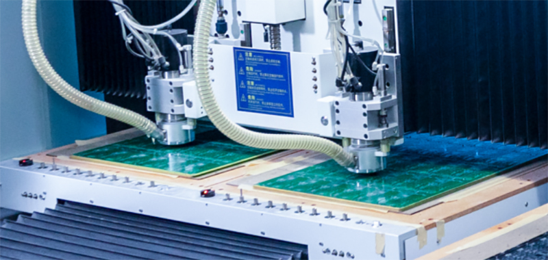
01. Molding board edge milling board
When the components are placed too close to the edge of the plate, the welding pad of the components will be milled out when the milling plate is formed. Generally, the distance between the welding pad and the edge should be greater than 0.2mm, otherwise the welding pad of the edge device will be milled out and the back assembly cannot weld the components.
02. Forming plate edge V-CUT
If the edge of the plate is a Mosaic V-CUT, the components need to be further away from the edge of the plate, because the V-CUT knife from the middle of the plate is generally more than 0.4mm away from the edge of the V-CUT, otherwise the V-CUT knife will hurt the welding plate, resulting in the components cannot be welded.
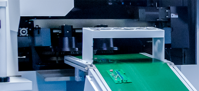
03. Component interference equipment
The layout of components too close to the edge of the plate during design may interfere with the operation of automatic assembly equipment, such as wave-soldering or reflow welding machines, when assembling components.
04. The device crashes into components
The closer a component is to the edge of the board, the greater its potential to interfere with the assembled device. For example, components such as large electrolytic capacitors, which are taller, should be placed farther away from the edge of the board than other components.
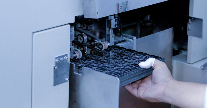
05. The components of the sub-board are damaged
After the product assembly is completed, the pieced product needs to be separated from the plate. During the separation, the components that are too close to the edge may be damaged, which may be intermittent and difficult to detect and debug.
The following is to share a production case about the edge device distance is not enough, resulting in damage to you ~
Problem description
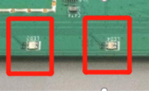
It is found that the LED lamp of a product is close to the edge of the board when SMT is placed, which is easy to be bumped in production.
Problem impact
Production and transportation, as well as the LED lamp will be broken when the DIP process passes the track, which will affect the function of the product.
Problem extension
It is necessary to change the board and move the LED inside the board. At the same time, it will also involve the change of the structural light guide column, causing a serious delay in the project development cycle.
Risk detection of edge devices
The importance of component layout design is self-evident, light will affect welding, heavy will directly lead to device damage, so how to ensure 0 design problems, and then successfully complete the production?
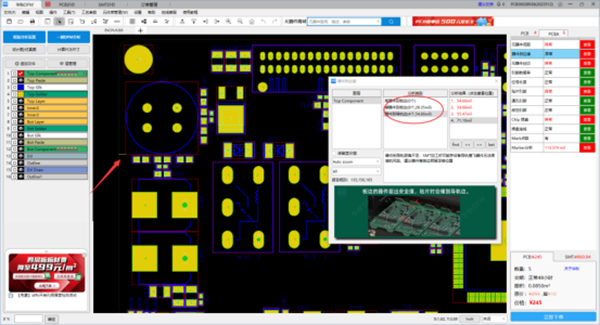
With the function of assembly and analysis,BEST can define inspection rules according to the parameters of the distance from the edge of the component type. It also has special inspection items for the layout of the components of the edge of the plate, including multiple detailed inspection items such as high device to the edge of the plate, low device to the edge of the plate, and device to the guide rail edge of the machine, which can fully meet the design requirements for the safe distance assessment of the device from the edge of the plate.
Post time: Apr-17-2023


