

The switching power ripple is inevitable. Our ultimate purpose is to reduce the output ripple to a tolerable level. The most fundamental solution to achieve this purpose is to avoid the generation of ripples. First of all And the cause.
With the switch of the SWITCH, the current in the inductance L also fluctuates up and down at the valid value of the output current. Therefore, there will also be a ripple that is the same frequency as Switch at the output end. Generally, the ripples of the riber refer to this, which is related to the capacity of the output capacitor and ESR. The frequency of this ripple is the same as the switching power supply, with a range of tens to hundreds of kHz.
In addition, Switch generally uses bipolar transistors or MOSFETs. No matter which one is, there will be a rise and decrease time when it is turned on and dead. At this time, there will be no noise in the circuit that is the same as the increase time as the Switch rising decrease time, or a few times, and is generally tens of MHz. Similarly, the diode D is in reverse recovery. The equivalent circuit is the series of resistance capacitors and inductors, which will cause resonance, and the noise frequency is tens of MHz. These two noise are generally called high -frequency noise, and the amplitude is usually much larger than the ripple.
If it is an AC / DC converter, in addition to the above two ripples (noise), there is also AC noise. The frequency is the frequency of input AC power supply, about 50-60Hz. There is also a co -mode noise, because the power device of many switching power supply uses the shell as a radiator, which produces an equivalent capacitance.
Measurement of switching power ripples
Basic requirements:
Coupling with an oscilloscope AC
20MHz bandwidth limit
Unplug the ground wire of the probe
1.AC coupling is to remove the superposition DC voltage and obtain an accurate waveform.
2. Opening the 20MHz bandwidth limit is to prevent the interference of high -frequency noise and prevent the error. Because the amplitude of high -frequency composition is large, it should be removed when measured.
3. Unplug the ground clip of the oscilloscope probe, and use the ground measurement measurement to reduce interference. Many departments do not have ground rings. But consider this factor when judging whether it is qualified.
Another point is to use a 50Ω terminal. According to the information of the oscilloscope, the 50Ω module is to remove the DC component and accurately measure the AC component. However, there are few oscilloscopes with such special probes. In most cases, the use of probes from 100kΩ to 10MΩ is used, which is temporarily unclear.
The above is the basic precautions when measuring the switching ripple. If the oscilloscope probe is not directly exposed to the output point, it should be measured by twisted lines or 50Ω coaxial cables.
When measuring high -frequency noise, the full band of the oscilloscope is generally hundreds of mega to GHz level. Others are the same as the above. Perhaps different companies have different test methods. In the final analysis, you must know your test results.
About oscilloscope:
Some digital oscilloscope cannot measure ripples correctly due to interference and storage depth. At this time, the oscilloscope should be replaced. Sometimes although the old simulation oscilloscope bandwidth is only tens of mega, the performance is better than the digital oscilloscope.
Inhibition of switching power ripples
For switching ripples, theoretically and actually exist. There are three ways to suppress or reduce it:
1. Increase the inductance and output capacitor filtering
According to the formula of the switching power supply, the current fluctuation size and inductance value of the inductive inductance become inversely proportional, and the output ripples and output capacitors are inversely proportional. Therefore, increasing electrical and output capacitors can reduce ripples.
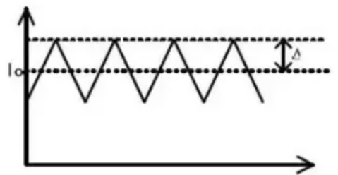
The picture above is the current waveform in the switching power supply inductor L. Its ripple current △ i can be calculated from the following formula:
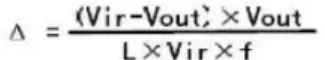
It can be seen that increasing L value or increasing the switching frequency can reduce the current fluctuations in the inductance.
Similarly, the relationship between output ripples and output capacitors: VRIPPLE = IMAX/(CO × F). It can be seen that increasing the output capacitor value can reduce the ripple.
The usual method is to use aluminum electrolytic capacitors for the output capacitance to achieve the purpose of large capacity. However, electrolytic capacitors are not very effective in suppressing high -frequency noise, and ESR is relatively large, so it will connect a ceramic capacitor next to it to make up for the lack of aluminum electrolytic capacitors.
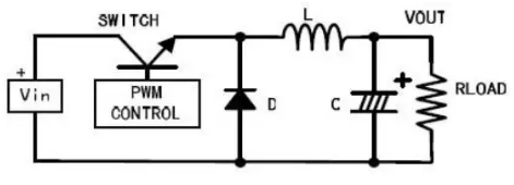
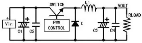
At the same time, when the power supply is working, the voltage VIN of the input terminal is unchanged, but the current changes with the switch. At this time, the input power supply does not provide a current well, usually near the current input terminal (taking the buck type as an example, is near Switch), and connects the capacitance to provide current.
After applying this countermeasure, the Buck switch power supply is shown in the figure below:
The above approach is limited to reducing ripples. Because of the volume limit, the inductance will not be very large; the output capacitor increases to a certain degree, and there is no obvious effect on reducing the ripples; the increase of the switching frequency will increase the switch loss. So when the requirements are strict, this method is not very good.
For the principles of switching power supply, you can refer to various types of switching power design manuals.
2. Two -level filtering is to add first -level LC filters
The inhibitory effect of the LC filter on the noise ripple is relatively obvious. According to the ripple frequency to be removed, select the appropriate inductor capacitor to form the filter circuit. Generally, it can reduce the ripples well. In this case, you need to consider the sampling point of the feedback voltage. (As shown below)
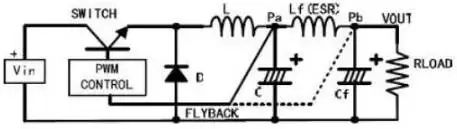
The sampling point is selected before the LC filter (PA), and the output voltage will be reduced. Because any inductance has a DC resistance, when there is a current output, there will be a voltage drop in the inductance, resulting in a decrease in the output voltage of the power supply. And this voltage drop changes with the output current.
The sampling point is selected after the LC filter (PB), so that the output voltage is the voltage we want. However, an inductance and a capacitor are introduced inside the power system, which may cause system instability.
3. After the output of the switching power supply, connect LDO filtering
This is the most effective way to reduce ripples and noise. The output voltage is constant and does not need to change the original feedback system, but it is also the most cost -effective and the highest power consumption.
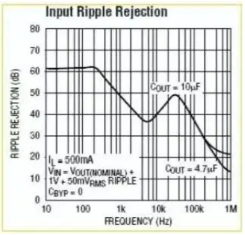
Any LDO has an indicator: noise suppression ratio. It is a frequency-DB curve, as shown in the figure below is the curve of LT3024 LT3024.
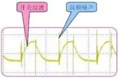
After LDO, the switching ripple is generally below 10mV. The following figure is the comparison of ripples before and after LDO:
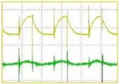
Compared with the curve of the figure above and the waveform on the left, it can be seen that the inhibitory effect of LDO is very good for the switching ripples of hundreds of KHz. But within a high frequency range, the effect of the LDO is not so ideal.
Reduce ripples. The PCB wiring of the switching power supply is also critical. For high -frequency noise, due to the large frequency of high frequency, although the post -stage filtering has a certain effect, the effect is not obvious. There are special studies in this regard. The simple approach is to be on the diode and the capacitance C or RC, or connect the inductance in series.
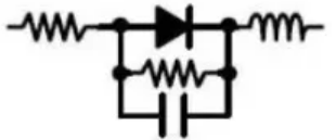
The above figure is an equivalent circuit of the actual diode. When the diode is high -speed, parasitic parameters must be considered. During the reverse recovery of the diode, the equivalent inductance and equivalent capacitance became an RC oscillator, generating high -frequency oscillation. In order to suppress this high -frequency oscillation, it is necessary to connect capacitance C or RC buffer network at both ends of the diode. The resistance is generally 10Ω-100 ω, and the capacitance is 4.7PF-2.2NF.
The capacitance C or RC on the diode C or RC can be determined by repeated tests. If it is not selected properly, it will cause more severe oscillation.
Post time: Jul-08-2023


