

Basic principles of PCB pad design
According to the analysis of solder joint structure of various components, in order to meet the reliability requirements of solder joints, PCB pad design should master the following key elements:
1, symmetry: both ends of the pad must be symmetrical, in order to ensure the balance of molten solder surface tension.
2. Pad spacing: Ensure the appropriate lap size of component end or pin and pad. Too large or too small pad spacing will cause welding defects.
3. Remaining size of the pad: the remaining size of the component end or pin after lapping with the pad must ensure that the solder joint can form a meniscus.
4.Pad width: It should be basically consistent with the width of the end or pin of the component.
Solderability problems caused by design defects
01. The size of the pad varies
The size of the pad design needs to be consistent, the length needs to be suitable for the range, the pad extension length has a suitable range, too short or too long are prone to the phenomenon of stele. The size of the pad is inconsistent and the tension is uneven.
02. The pad width is wider than the pin of the device
Pad design can not be too wide than the components, the width of the pad is 2mil wider than the components. Too wide pad width will lead to component displacement, air welding and insufficient tin on the pad and other problems.
03. Pad width narrower than device pin
The width of the pad design is narrower than the width of the components, and the area of the pad contact with the components is less when SMT patches, which is easy to cause the components to stand or turn over.
04. The length of the pad is longer than the pin of the device
The designed pad should not be too long than the pin of the component. Beyond a certain range, excessive flux flow during SMT reflow welding will cause the component to pull the offset position to one side.
05. The spacing between the pads is shorter than that of the components
The short-circuit problem of pad spacing generally occurs in the IC pad spacing, but the inner spacing design of other pads can not be much shorter than the pin spacing of components, which will cause short circuit if it exceeds a certain range of values.
06. Pin width of pad is too small
In the SMT patch of the same component, defects in the pad will cause the component to pull out. For example, if a pad is too small or part of the pad is too small, it will form no tin or less tin, resulting in different tension at both ends.
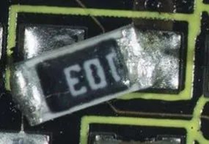
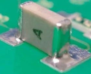
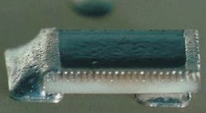
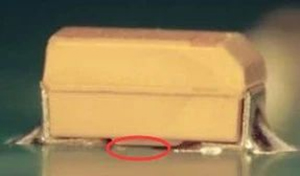
Real cases of small bias pads
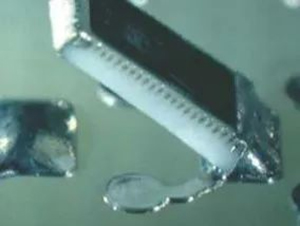
The size of the material pads does not match the size of the PCB packaging
Problem description: When a certain product is produced in SMT, it is found that the inductance is offset during the background welding inspection. After verification, it is found that the inductor material does not match the pads. *1.6mm, the material will be reversed after welding.
Impact: The electrical connection of the material becomes poor, affects the performance of the product, and seriously causes the product to be unable to start normally;
Extension of the problem: If it cannot be purchased to the same size as the PCB pad, the sensor and current resistance can meet the materials required by the circuit, then the risk of changing the board.
Post time: Apr-17-2023


