

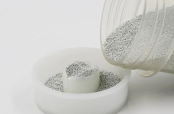
When discussing solder beading, we first need to accurately define the SMT defect. The tin bead is found on a reflow welded plate, and you can tell at a glance that it is a large tin ball embedded in a pool of flux positioned next to discrete components with very low ground height, such as sheet resistors and capacitors, thin small profile packages (TSOP), small profile transistors (SOT), D-PAK transistors, and resistance assemblies. Because of their position in relation to these components, tin beads are often referred to as "satellites".
Tin beads not only affect the appearance of the product, but more importantly, due to the density of components on the printed plate, there is a danger of short circuit of the line during use, thus affecting the quality of electronic products. There are many reasons for the production of tin beads, often caused by one or more factors, so we must do a good job of prevention and improvement in order to better control it. The following article will discuss the factors that affect the production of tin beads and the countermeasures to reduce the production of tin beads.
Why do tin beads occur?
Simply put, tin beads are usually associated with too much solder paste deposition, because it lacks a "body" and is squeezed under discrete components to form tin beads, and the increase in their appearance can be attributed to the increase in the use of rinsed-in solder paste. When the chip element is mounted into the rinseable solder paste, the solder paste is more likely to squeeze under the component. When the deposited solder paste is too much, it is easy to extrusion.
The main factors affecting the production of tin beads are:
(1) Template opening and pad graphic design
(2) Template cleaning
(3) Repetition accuracy of the machine
(4) Temperature curve of reflow furnace
(5) Patch pressure
(6) solder paste quantity outside the pan
(7) The landing height of tin
(8) Gas release of volatile substances in the line plate and solder resistance layer
(9)Related to flux
Ways to prevent the production of tin beads:
(1) Select the appropriate pad graphics and size design. In the actual pad design, should be combined with PC, and then according to the actual component package size, welding end size, to design the corresponding pad size.
(2) Pay attention to the production of steel mesh. It is necessary to adjust the opening size according to the specific component layout of the PCBA board to control the printing amount of solder paste.
(3) It is recommended that PCB bare boards with BGA, QFN and dense foot components on the board take strict baking action. To ensure that the surface moisture on the solder plate is removed to maximize weldability.
(4) Improve the quality of template cleaning. If the cleaning is not clean. Residual solder paste at the bottom of the template opening will accumulate near the template opening and form too much solder paste, causing tin beads
(5) To ensure the repeatability of the equipment. When the solder paste is printed, due to the offset between the template and the pad, if the offset is too large, the solder paste will be soaked outside the pad, and the tin beads will easily appear after heating.
(6) Control the mounting pressure of the mounting machine. Whether the pressure control mode is attached, or the component thickness control, the Settings need to be adjusted to prevent tin beads.
(7)Optimize the temperature curve. Control the temperature of reflow welding, so that the solvent can be volatilized on a better platform.
Don't look at the "satellite" is small, one can not be pulled, pull the whole body. With electronics, the devil is often in the details. Therefore, in addition to the attention of process production personnel, relevant departments should also actively cooperate, and communicate with process personnel in time for material changes, replacements and other matters to prevent changes in process parameters caused by material changes. The designer responsible for PCB circuit design should also communicate with the process personnel, refer to the problems or suggestions provided by the process personnel and improve them as much as possible.
Post time: Jan-09-2024


