

Understand DIP
DIP is a plug-in. Chips packaged in this way have two rows of pins, which can be directly welded to chip sockets with DIP structure or welded to welding positions with the same number of holes. It is very convenient to realize PCB board perforation welding, and has good compatibility with the motherboard, but because of its packaging area and thickness are relatively large, and the pin in the process of insertion and removal is easy to be damaged, poor reliability.
DIP is the most popular plug-in package, the application range includes standard logic IC, memory LSI, microcomputer circuits, etc. Small profile package (SOP), derived from SOJ (J-type pin small profile package), TSOP (thin small profile package), VSOP (very small profile package), SSOP (reduced SOP), TSSOP (thin reduced SOP) and SOT (small profile transistor), SOIC (small profile integrated circuit), etc.
DIP device assembly design defect
The PCB package hole is larger than the device
PCB plug-in holes and package pin holes are drawn in accordance with the specifications. Due to the need for copper plating in the holes during plate making, the general tolerance is plus or minus 0.075mm. If the PCB packaging hole is too large than the pin of the physical device, it will lead to the loosening of the device, insufficient tin, air welding and other quality problems.
See the figure below, using WJ124-3.81-4P_WJ124-3.81-4P (KANGNEX) device pin is 1.3mm, PCB packaging hole is 1.6mm, aperture is too large lead to over wave welding space time welding.
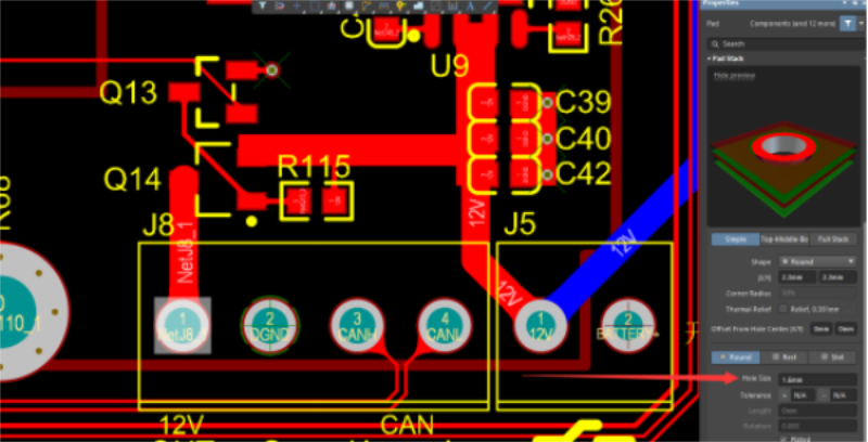
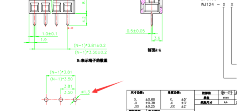
Attached to the figure, purchase WJ124-3.81-4P_WJ124-3.81-4P (KANGNEX) components according to the design requirements, pin 1.3mm is correct.
PCB package hole is smaller than the device
Plug-in, but will hole no copper, if it is single and double panels can use this method, single and double panels are outer electrical conduction, solder can be conductive; The plug-in hole of multilayer board is small, and PCB board can only be remade if the inner layer has electrical conduction, because the inner layer conduction cannot be remedied by reaming.
As shown in the figure below, components of A2541Hwv-3P_A2541HWV-3P (CJT) are purchased according to the design requirements. The pin is 1.0mm, and the PCB sealing pad hole is 0.7mm, resulting in the failure to insert.
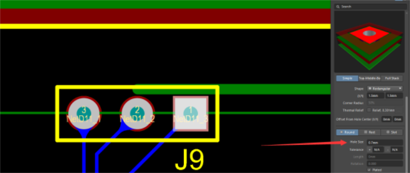
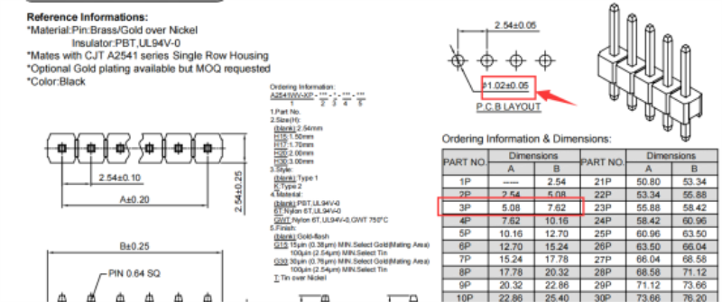
The components of A2541Hwv-3P_A2541HWV-3P (CJT) are purchased according to the design requirements. The pin 1.0mm is correct.
Package pin spacing differs from device spacing
The PCB sealing pad of the DIP device not only has the same aperture as the pin, but also needs the same distance between the pin holes. If the spacing between the pin holes and the device is inconsistent, the device cannot be inserted, except for the parts with adjustable foot spacing.
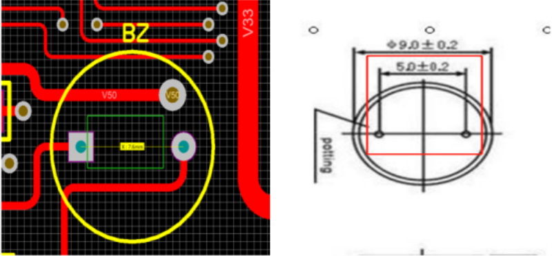
As shown in the figure below, the pin hole distance of PCB packaging is 7.6mm, and the pin hole distance of purchased components is 5.0mm. The difference of 2.6mm leads to the device being unusable.
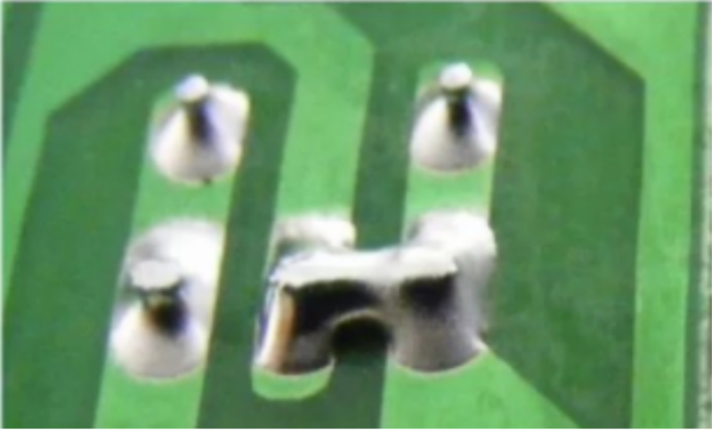
The PCB packaging holes are too close
In PCB design, drawing and packaging, it is necessary to pay attention to the distance between pin holes. Even if the bare plate can be generated, the distance between pin holes is small, it is easy to cause tin short circuit during assembly by wave soldering.
As shown in the figure below, short circuit may be caused by small pin distance. There are many reasons for short circuit in soldering tin. If the assemblability can be prevented in advance at the design end, the incidence of problems can be reduced.
DIP device pin problem case
Problem description
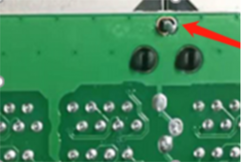
After wave crest welding of a product DIP, it was found that there was a serious shortage of tin on the solder plate of the fixed foot of the network socket, which belonged to air welding.
Problem impact
As a result, the stability of the network socket and PCB board becomes worse, and the force of the signal pin foot will be exerted during the use of the product, which will eventually lead to the connection of the signal pin foot, affecting the product performance and causing the risk of failure in the use of users.
Problem extension
The stability of the network socket is poor, the connection performance of the signal pin is poor, there are quality problems, so it may bring security risks to the user, the ultimate loss is unimaginable.
DIP device assembly analysis check
There are many problems related to DIP device pins, and many key points are easy to be ignored, resulting in the final scrap board. So how to quickly and completely solve such problems once and for all?
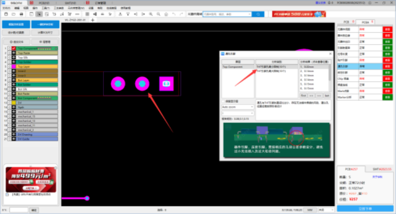
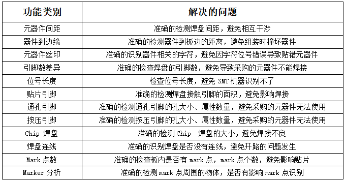
Here, the assembly and analysis function of our CHIPSTOCK.TOP software can be used to conduct special inspection on the pins of DIP devices. The inspection items include the number of pins through holes, the large limit of THT pins, the small limit of THT pins and the attributes of THT pins. The inspection items of pins basically cover the possible problems in the design of DIP devices.
After the completion of PCB design, PCBA assembly analysis function can be used to discover design defects in advance, solve design anomalies before production, and avoid design problems in the assembly process, delay production time and waste research and development costs.
Its assembly analysis function has 10 major items and 234 fine items inspection rules, covering all possible assembly problems, such as device analysis, pin analysis, pad analysis, etc., which can solve a variety of production situations that engineers cannot anticipate in advance.
Post time: Jul-05-2023


