


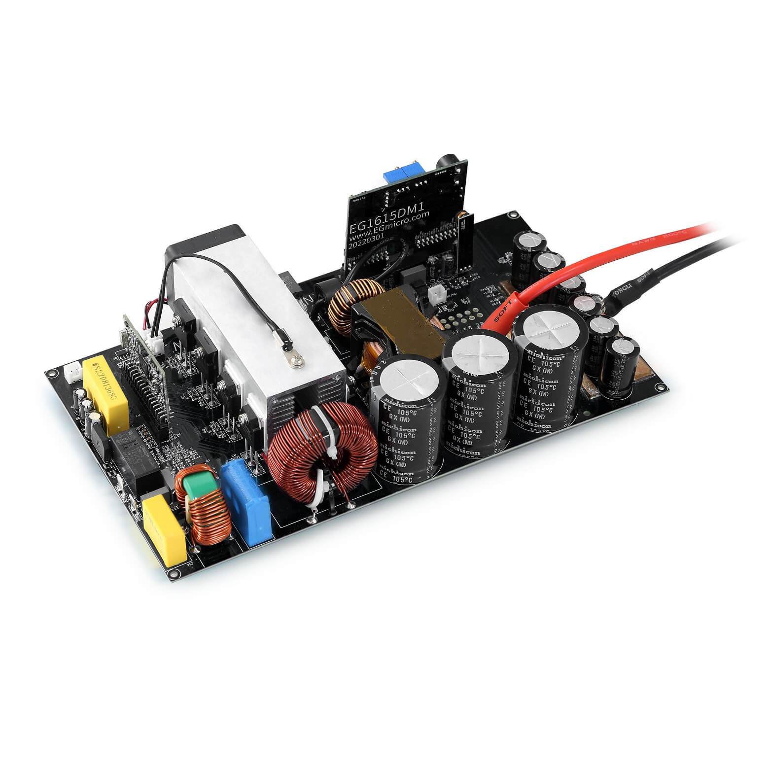
High quality ENIG PCB for medical equiment Aerospace military defense area Gold thickness 1u”-3u”
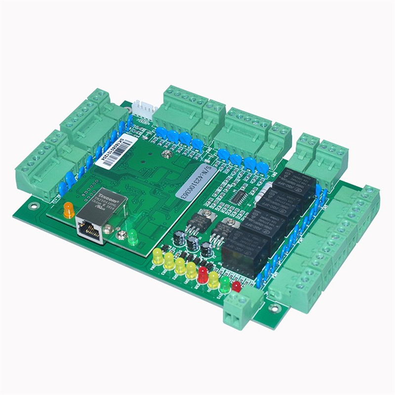
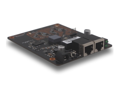
We are manufacture pcb and pcb assembly one-stop service factories. have 400peoples total. 20% increase sales volume each year. 70% production all from overseas. we make 1-12layer.FR4.CEM-1.CEM-3.HDI. AL material. we are welcome prototypes orders. normal pcb samples about 3days can deliverywe can send to your withine 12hour or 24hour pay urgent costs. pcba prototypes about 1day can delivery. smt and dip and by hand components all can do. include 0201 components.BGA. 100%Quality promise. because of Fly probe. E-testing shelf.X-RAY.AOI. Function testing for each board. we can make design layout or copy the board if no pcb gerber file and bom list. you can send your previours true sample to us if have. please provide shematic diagram. outline size. parts datasheet if no true samples. we sure repair or reproduce or bear the quality problems costs if quality make our sides. any answer will be reply withine 5hour. we have ISO9001.TS16949.SGS.UL. ROHS certification. Looking forwarder to hear from your soon. welcome your offer soon.
Technical parameters
•Material:FR-4,CEM-3,CEM-1,AL ,HDI, Halogen-free , Ceramic boards
•Min Solder Mask bridge:0.1mm
•Min/max Solder Mask thickness:10um-25um
•Min hold solder diameter:0.1mm(single side)
•Diameter Tolerance:PTH ±0.076mm NPTH ±0.05mm
•Tenting by Mask (yes/no):Yes
•Layer Counts:1-12 LAYERS
•Board Thickness:0.4mm—3.5mm
•Thickness Tolerance( t≥0.8mm):0.8 +/-0.1mm;1.2-1.6 +/-0.13mm;2.4 +/-0.18mm;3.2 +/-0.25mm
•Thickness Tolerance( T<0.8mm):0.4-0.6 +/-0.1mm
•Minimum Line (0,5OZ):0.10mm(for plating gold):Minimum Space (0,5OZ)0.10mm(for plating gold)
•Minimum Line (1OZ):0.15mm:Minimum Line (2OZ):0.20mm
•Minimum Line (3OZ):0.25mm:Minimum Space (1OZ):0.15mm
•Minimum Space (2OZ):0.20mm
•Minimum Space (3OZ):0.25mm
•Out Layer Copper Thickness:0.5-2OZ
•Inner Layer Copper Thickness:0.5-2OZ
•Min Drilling Hole(Finished):0.25mm
•Annular ring:0.1mm Registration:±0.1mm
•Aspect Ratio:Through Holes - 8:1
•Solder Mask color:Green, black, red, white. Mini. Solder Mask Clearance:0.05mm
•Legend color:Green, white, red, yellow, black.
•Maximum Board Size:500x600mm
•Twist and Bow (for SMT assemble):≤0.75%
Thickness Tin/Lead HASL:5-25um

Material: FR-41.6T1/1/1/1 OZ
Minimum line width /
Line distance: 6/6mil
Minimum aperture: 0.3mm
surface finished : black masking oil nickel gold 6Layers
Application: Home appliance control motherboard
Material: FR-41.6T1/1/1 OZ
Minimum line width / Line distance: 4/4mi1
Minimum aperture /
Minimum BGA: 0.25mm/0.25*0.25mm
surface finished : blue masking oil nickel gold 6Layers
Product Use: iRobot navigation board

Products categories


-

Phone
-

E-mail
-

Whatsapp
-

Skype
-

Skype
-

Skype