

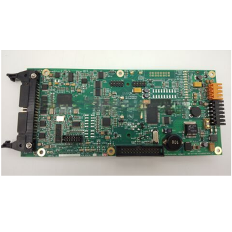


Controlling Printed Circuit Board Manufacturing PCBA Assembly Customized DIP/SMT Circuit Boards

- Customized Multilayer SMT PCBA Manufacturing Prototype PCB assembly service
PCBA, short for printed circuit board assembly, refers to the combination of PCB, components and electronic accessories. Simply speaking, PCBA is actually the PCB with components assembled. This article provides a comprehensive introduction of PCBA from which everybody will learn much.
Actual PCBA process steps:
Step 1: Solder Paste Stenciling
Step 2: Pick and Place
Step 3: Reflow Soldering
Step 4: Inspection and Quality Control
Step 5: Through-Hole Component Insertion
Step 6: Final Inspection and Functional Test
-PCBA OEM &ODM services
-Components sourcing
-Plastic and metal casing design&production services
-PCBA assembly (SMT, DIP, MI, AI)
-PCBA testing (AOI testing, ICT testing, functional testing)
-Burn-in testing
-Turnkey assembly and final testing(including plastic,metal casing,PCBA motherboard,cables,switches and other components, etc.)
-Logistics arrangements, importing and exporting goods from China
-Dust-Free workshop
-Perfect quality guarantee such as ISO9001:2008,ISO13485:2016 & IATF16949:2016 and ROHS& UL certified;
| Layer: | 1-40 layer |
| Surface: | HASL/OSP/ENIG/ImmersionGold/Flash Gold/Gold finger ect. |
| Copper thickness: | 0.25 Oz -12 Oz |
| Material: | FR-4,Halogen free,High TG,Cem-3,PTFE,Aluminum BT,Rogers |
| Board thickness | 0.1 to 6.0mm(4 to 240mil) |
| Minimum line width/space | 0.076/0.076mm |
| Minimum line gap | +/-10% |
| Outer layer copper thickness | 140um(bulk) 210um(pcb prototype) |
| Inner layer copper thickness | 70um(bulk) 150um(pcb protytype) |
| Min.finished hole size(Mechanical) | 0.15mm |
| Min.finished hole size (laser hole) | 0.1mm |
| Solder Mask Color | Green,Blue,Black,White,Yellow,Red,Grey |
| Delivery time | Mass:10~12d/ Sample:5~7D |
| Capacity | 35000sq/m |
| Certification: | ISO9001:2015, ISO13485:2016, IAFT16949:2016 |
We are a one-stop electronic manufacturing service provider headquartered in Shenzhen, China. We build long lasting, mutually beneficial relationships with our customers through hard work, integrity, communication, and honesty. Whether you are looking for production or prototype PCB assembly services, we are here to help. Please contact us today to learn more.
- Quick Turn: Get your printed circuit boards assembled quickly without compromise.
- Prototype: Small and medium prototype pcb runs before moving in to production.
- Production: Large production pcba runs with the highest quality and yield.
- Electronics Product Development: Electronics hardware product development services from concept to manufacturing.
- Turnkey: Bare board fabrication, component sourcing, and assembly labor. PCBAs are shipped ready to go.
- Consigned: Provide us with bare boards and/or components and we will take care of the assembly labor.
- Partially Kitted: Provide a few hard to find components and we'll return what isn't used with the assemblies.
- Box Build: Let our mechanical assembly team integrate your PCBA into your final packaging.
- Cable/Wire Harness: Cable and wire stripping, crimping, and precision cutting to your exact specifications.
- Functional Testing: Functionally test your PCBAs with your provided test documentation and equipment.
Products categories
-
New energy PCB Printed circuit boards used in s...
-
MX-6924 F5 Qualcomm QCN9024/5GHz/4×4 MIMO/...
-

F405V2DJI Flight controller Dual BEC barometer ...
-

2-bit 60AF405 V2 DJI twin BEC gyroscope baromet...
-
Jetson Xavier NX Development Kit AI Intelligent...
-

35A F405 mini DJI Fly tower 2-6S FPV crossover ...
-

Phone
-

E-mail
-

Whatsapp
-

Skype
-

Skype
-

Skype