One-stop Electronic Manufacturing Services, help you easily achieve your electronic products from PCB & PCBA

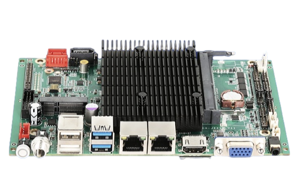
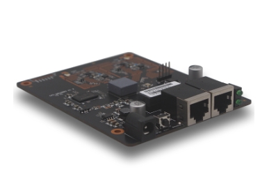
Car charging pile motherboard control board SMT chip processing PCBA processing Charging pile solution circuit board manufacturer

Short Description:

The car charging pile PCBA motherboard is the core component used to control the charging pile.
It has a variety of functions. Here is a brief introduction to its main features:
Powerful processing capability: The PCBA motherboard is equipped with a high-performance microprocessor, which can quickly handle various charging control tasks and ensure the safety and stability of the charging process.
Rich interface design: PCBA motherboard provides a variety of interfaces, such as power interfaces, communication interfaces, etc., which can meet the data transmission and signal interaction needs between charging piles, vehicles and other equipment.
Intelligent charging control: The PCBA motherboard can intelligently control the charging current and voltage according to the battery power status and charging needs to avoid battery overcharging or undercharging, effectively extending battery life.
Complete protection functions: The PCBA motherboard integrates a variety of protection functions, such as over-current protection, over-voltage protection, under-voltage protection, etc., which can cut off the power supply in time when abnormal conditions occur to ensure the normal operation of the system. Safety of the charging process.
Energy saving and environmental protection: The PCBA motherboard adopts an energy-saving design, which can adjust the power supply current and voltage according to actual needs, effectively reducing energy consumption and reducing the impact on the environment.
Easy to maintain and upgrade: PCBA motherboard has good scalability and compatibility, which facilitates later maintenance and upgrades, and can adapt to changes in different models and different charging needs.


Product Detail

Product Tags

Demonstration of process capabilities:
1. Plate thickness:
0.3MM~3.0MM (minimum 0.15mm, maximum thickness can be made according to customer requirements)
2. Ink:
Green oil, blue oil, black oil, white oil, butter red oil, purple, matte black
3. Surface technology: Anti-oxidation (SOP), leaded tin spray, lead-free tin spray, immersion gold, gold plating, silver plating, nickel plating, gold finger, carbon oil
4. Special technology: impedance board, high frequency board, buried blind hole board (minimum hole 0.1mm laser hole)

Model: customized
Number of product layers: multi-layer
Insulating material: organic resin
Flame retardant performance: VO board
Reinforcement material: fiberglass cloth base
Mechanical rigidity: rigid
Material: copper
Insulation layer thickness: thin plate
Processing technology: Calendered foil
Insulating resin: polyimide resin (PI)
Number of production layers: 1~10 layers
Maximum size: 600X600mm
Minimum size: ±0.15mm
Layman’s tolerance: 0.4~3.2mm
Plate thickness specification: ±10%
Board limit line width: 5MIL (0.127mm)
Board limit line distance: 5MIL (0.127mm)
Finished copper thickness: 1OZ (35UM)
Mechanical drilling: 0.25~6.3mm
Aperture tolerance: ±0.075mm
Minimum character: width ≥ 0.15mm/height ≥ 0.85n
Distance from line to outline: ≥12MIL (0.3mm)
Solder mask type: photosensitive ink/matte ink
No spacing panel: Omm
Panel spacing: 1.5mm
​One-stop PCBA service, fast delivery.


  • Previous:
  • Next:

  • Write your message here and send it to us