

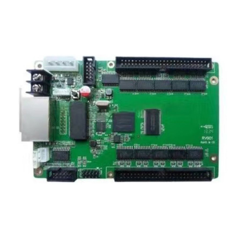
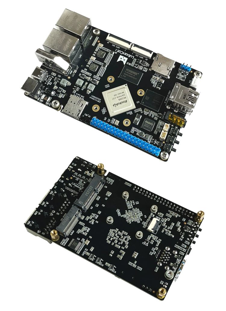
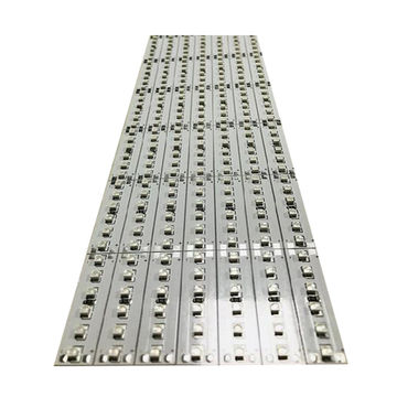
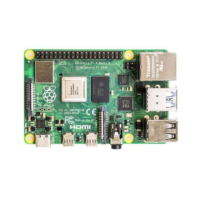
OEM PCBA Clone Assembly Service Other PCB & PCBA Custom Electronics PCB Circuit Board
Specification
PCB Technical Capacity
Layers Mass production: 2~58 layers / Pilot run: 64 layers
Max. Thickness Mass production: 394mil (10mm) / Pilot run: 17.5mm
Materials FR-4 (Standard FR4, Mid-Tg FR4,Hi-Tg FR4, Lead free assembly material) , Halogen-Free, Ceramic filled , Teflon, Polyimide, BT,PPO,PPE, Hybrid, Partial hybrid, etc
Min. Width/Spacing Inner layer: 3mil/3mil (HOZ), Outer layer: 4mil/4mil(1OZ)
Max. Copper Thickness 6.0 OZ / Pilot run: 12OZ
Min. Hole Size Mechanical drill: 8mil(0.2mm) Laser drill: 3mil(0.075mm)
Surface Finish HASL,Immersion Gold, Immersion Tin, OSP, ENIG + OSP, Immersion , ENEPIG, Gold Finger
Special Process Buried Hole, Blind Hole, Embedded Resistance, Embedded Capacity, Hybrid, Partial hybrid, Partial high density, Back drilling, and Resistance control
PCBA technical Capacity
Advantages ----Professional Surface-mounting and Through-hole soldering technology
----Various sizes like 1206,0805,0603 components SMT technology
----ICT(In Circuit Test),FCT(Functional Circuit Test)
----PCB Assembly With UL,CE,FCC,Rohs Approval
----Nitrogen gas reflow soldering technology for SMT.
----High Standard SMT&Solder Assembly Line
----High density interconnected board placement technology capacity.
Components Passive Down to 0201 size, BGA and VFBGA, Leadless Chip Carriers/CSP
Double-sided SMT Assembly, Fine Pitch to 0.8mils, BGA Repair and Reball
Testing Flying Probe Test,X-ray Inspection AOI Test
| SMT Position accuracy | 20 um |
| Components size | 0.4×0.2mm(01005) —130×79mm, Flip-CHIP, QFP, BGA, POP |
| Max. component height | 25mm |
| Max. PCB size | 680×500mm |
| Min. PCB size | no limited |
| PCB thickness | 0.3 to 6mm |
| Wave-Solder Max. PCB width | 450mm |
| Min. PCB width | no limited |
| Component height | Top 120mm/Bot 15mm |
| Sweat-Solder Metal type | part, whole, inlay, sidestep |
| Metal material | Copper, Aluminum |
| Surface Finish | plating Au, , plating Sn |
| Air bladder rate | less than 20% |
| Press-fit Press range | 0-50KN |
| Max. PCB size | 800X600mm |


-

Phone
-

E-mail
-

Whatsapp
-

Skype
-

Skype
-

Skype